2022 Semiconductor Wafer Industry Overview
2022 Semiconductor Wafer Industry Overview
Semiconductor silicon wafer is the carrier for manufacturing chips, also known as silicon wafer because the raw material is silicon.
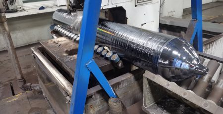
After planning and management-free silicon refining, purification, monocrystalline silicon production, wafer forming and other processes, it can enter the subsequent links such as chip single-channel etching, which is the most important pre-process for chip manufacturing.
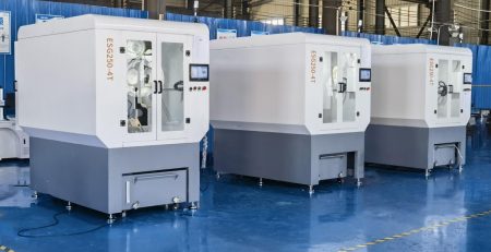
The concept mainly includes: companies that develop and manufacture semiconductor wafers, silicon wafers and polished wafers.

Classified by process
According to the type of process, it can be divided into polished wafer, epitaxial wafer and SOI wafer. Among them, polished wafers and epitaxial wafers are the mainstream products in the market, and SOI silicon wafers are mainly used in special application fields such as RF front-end.
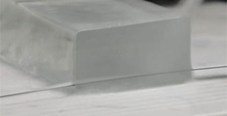
Polishing sheet: It is formed by mixing nano-scale silica particles with high-efficiency binder, and then uniformly coating the surface of polyester film, drying and curing reaction.
Epitaxial Wafer: Epitaxy is a type of semiconductor process. In the bipolar process, the bottom layer of the silicon wafer is the P-type substrate silicon (some add a buried layer); Then a layer of single crystal silicon is grown on the substrate, which is called the epitaxial layer; and then the base region, the emitter region, etc. are implanted on the epitaxial layer.
Finally, the vertical NPN tube structure is basically formed: the epitaxial layer is the collector region, and the epitaxial layer has the base region and the emitter region. An epitaxial wafer is a silicon wafer with an epitaxial layer on a substrate.
SOI: The full name is Silicon-On-Insulator, which is silicon on an insulating substrate. This technology introduces a buried oxide layer between the top silicon and the back substrate.
Sort by size
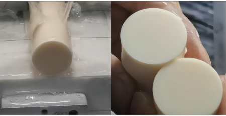
Generally, the diameter of the silicon wafer is used to distinguish the specifications, usually 6 inches, 8 inches and 12 inches. At present, the size of semiconductor silicon wafers has been continuously developing to large sizes. Larger diameter semiconductor wafers can reduce the average production cost per chip, thus providing higher economies of scale. However, due to the high purity of large-sized silicon wafers, technology development and large-scale production are difficult, and it is necessary to improve the production process and improve the performance of the equipment.
Driven by industries such as 5G mobile phones, high-performance computing, vehicle electrification and intelligence, and the Internet of Things, 8-inch and 12-inch silicon wafers have become mainstream. In Q4 2021, 8-inch silicon wafer shipments will be 6 million pieces/month, and 12-inch silicon wafer shipments will exceed 7.5 million pieces/month.
Global 8-inch silicon wafer shipments (thousands/month)

Global 12-inch silicon wafer shipments (thousands/month)

Classified by use
According to the application scenarios of silicon wafers, silicon wafers can be divided into positive film, auxiliary film and time electrode. Positive films can be used directly in wafer fabrication. Accompanying film can be divided into test film, blank film and control film according to the function.
The test piece is used to experiment and check the state of the initial operation of the manufacturing equipment to improve its stability. Baffles are used for commissioning of new production lines and to protect genuine products during wafer production. Chip control is to test and monitor the yield of new processes before formal production.

Semiconductor wafer industry chain

Semiconductor wafers are an important upstream industry. Semiconductor manufacturing enterprises obtain semiconductor silicon wafer products after processing crystalline silicon raw materials. Semiconductor wafer products are provided to midstream companies that produce photovoltaic cells and photovoltaic modules. Finally, the midstream enterprises will provide them to downstream enterprises whose main business is photovoltaic application products.