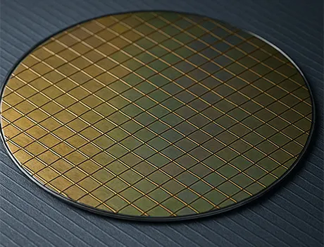
Semiconductor wafer slicing is a critical IC manufacturing step where precision and surface integrity determine device yield.
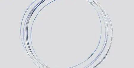
A diamond cutting wire loop is a closed loop of diamond-coated wire that slices ingots with ultra-precise, minimal kerf loss.
Its key advantages are lower thermal and mechanical stress than laser or blade cutting, which matters most as wafers get thinner.
Semiconductor wafer slicing is a critical process in the manufacturing of integrated circuits (ICs) and other microelectronic devices. Precision and efficiency are paramount, as even minor defects can lead to significant performance issues in the final product. Among the various cutting technologies available, diamond cutting wire loop has emerged as a superior method due to its exceptional accuracy, minimal material loss, and extended tool life.
In this article, we will explore why diamond wire cutting is becoming the preferred choice for semiconductor wafer dicing and how it outperforms traditional methods like blade sawing and laser cutting.
The Challenges of Semiconductor Wafer Cutting
Semiconductor wafers, typically made of silicon, are extremely thin and fragile. The cutting process must ensure high precision with minimal kerf width and chipping, low thermal damage to prevent microcracks, and high throughput for cost-effective production.
Traditional methods such as mechanical blade sawing can cause microcracks and material loss, while laser cutting may introduce thermal stress. This is where diamond cutting wire loop technology excels.
What Is Diamond Cutting Wire Loop?
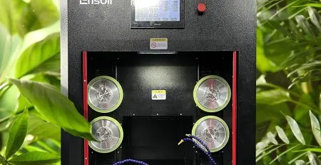
Application Lab
Send us your material — get a free test-cut report
Tell us the material, thickness and target tolerance. We cut a sample on our own diamond wire saw and return wire spec, feed rate, surface finish and cycle time.
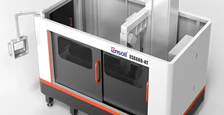
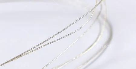
A diamond cutting wire loop is a thin, flexible wire embedded with diamond abrasive particles. It operates by continuously moving the wire across the wafer, enabling precise and smooth cuts with minimal mechanical stress. .
Key Advantages of Diamond Wire Cutting
Ultra-Precise Cutting with Minimal Kerf Loss
Diamond wire cutting produces an extremely narrow kerf, as small as 20-30 µm, allowing for higher wafer yield compared to blade sawing. The fine abrasive action reduces chipping and edge defects, crucial for delicate wafers.
Reduced Material Waste
Since the wire is much thinner than a saw blade, less silicon is wasted, improving material utilization and lowering production costs.
Lower Thermal and Mechanical Stress
Unlike laser cutting, diamond wire cutting generates minimal heat, preventing thermal damage to the wafer. The process applies uniform pressure, reducing the risk of microcracks.
Longer Tool Life and Lower Maintenance
Diamond is one of the hardest materials, ensuring durability and consistent performance over extended use. Unlike blades that wear out quickly, diamond wire maintains sharpness for longer, reducing downtime for replacements.
Versatility in Cutting Various Materials
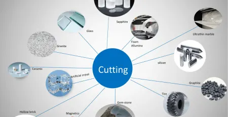
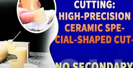
Besides silicon wafers, diamond wire loops can cut gallium arsenide (GaAs), sapphire, and ceramic substrates with high precision.
Applications in Semiconductor Manufacturing
Diamond wire cutting is widely used in wafer dicing for separating individual chips from a wafer, thin wafer processing for advanced 3D IC stacking, and solar cell manufacturing for cutting silicon ingots into wafers.
Conclusion
The diamond cutting wire loop method offers unparalleled advantages in semiconductor wafer cutting, including higher precision, reduced waste, lower stress, and longer tool life. As the demand for thinner and more efficient wafers grows, this technology is set to become the industry standard.
Manufacturers looking to improve yield and reduce costs should consider adopting diamond wire cutting for their wafer dicing processes. With continuous advancements in wire technology, we can expect even greater efficiency and performance in the future.
Would you like to learn more about how diamond wire cutting can optimize your semiconductor production? Let us discuss in the comments!
Frequently Asked Questions
What is a diamond cutting wire loop?
It is a closed loop of high-tensile wire electroplated or resin-bonded with diamond grit, used to slice semiconductor ingots into wafers with very narrow kerf loss.
Last reviewed: September 2026
Why is kerf loss important in wafer cutting?
Kerf is the silicon removed by the cut itself. Minimizing it means more wafers per ingot, which is the largest cost lever in wafer manufacturing.
Why does diamond wire loop cause less damage than other methods?
It cuts by cold mechanical micro-grinding under coolant, so it introduces neither a heat-affected zone nor high mechanical stress into the wafer.
Key Takeaways
Traditional cutting methods suffer four pain points: slow processes, heavy material loss, limited material range, and operator safety risks.
The... read more
The photovoltaic and semiconductor industries are built on precision. Every micron matters when crafting silicon wafers, where material integrity directly... read more
Efficient material cutting methods play a pivotal role in various industries, impacting productivity and quality significantly. In this blog post,... read more
The optics industry demands extreme precision, whether for wafer-level optics production, microscope slide preparation, or custom optical glass cutting... read more
Key Takeaways
Craft cutters such as Silhouette machines only handle flexible rubber-bonded magnets up to about 1 mm thick; sintered NdFeB,... read more
Introduction
Hard and brittle materials are essential in industries like electronics, optics, aerospace, and medical devices. However, cutting them often... read more