Fluxo de Processamento de Lingote de Silício de Cristal Único
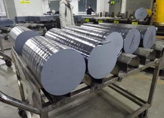
- Um lingote de silício monocristalino passa por corte, Moagem de diâmetro, Cortar, Chanframento de borda, Lapeamento e polimento antes de estar pronto para litografia.
- A precisão da superfície na fase de corte determina quanto trabalho de planarização a jusante é necessário.
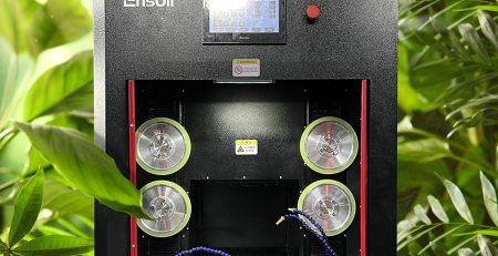
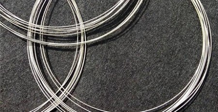
- O corte com fio de diamante é a forma padrão de transformar um lingote em pastilhas nuas com variação de espessura reduzida e baixo dano subsuperficial.
Na etapa de preparação do wafer de silício monocristal, Os lingotes de silício monocristalino precisam ser processados em pastilhas de silício cruas ou pastilhas nuas com alta precisão de superfície e qualidade de superfície para se preparar para a planarização, litografia e outros processos na primeira fase do processo de CI. Superfície de substrato ultra-lisa e sem danos é necessária aqui.
Para pastilhas de silício com diâmetro de ≤200 mm, O processo tradicional de processamento de wafer de silício é:
crescimento de cristal único → corte → diâmetro externo moagem de barril → borda plana ou tratamento de ranhura em V → wafering → chanfro → moagem → gravação → polimento → limpeza → embalagem .

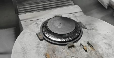
Retificação de diâmetro externo: Since the outer diameter surface of the single crystal silicon rod is not flat and the diameter is larger than the specified diameter specification of the final polished wafer, Um diâmetro mais preciso pode ser obtido por laminação de diâmetro externo.
Processamento de borda plana ou ranhura em V: Ele é especificado para ser processado no plano de referência, and the flat edge or V-groove with a specific crystallographic direction on the silício monocristalino holder.
Bolacha: refere-se ao corte de uma haste de silício de cristal único em fatias finas com dimensões geométricas precisas.
Chanfrando: refere-se ao corte da borda afiada do wafer cortado em forma de arco para evitar rachaduras na borda do cavaco e defeitos de qualidade
Esmerilhação: refere-se à remoção de marcas de serra e camadas de danos superficiais causados por fatiamento e retificação por retificação, Alterando efetivamente o empenamento, Planicidade e paralelismo de um wafer de silício de produto único, e atingir as especificações que podem ser tratadas por um processo de polimento.
Perguntas Frequentes
What are the main steps in single-crystal silicon ingot processing?
The typical flow is cropping to length, grinding to precise diameter, slicing into wafers, Chanframento de borda, then lapping, etching and polishing to reach the surface quality lithography requires.
Why is slicing done with diamond wire?
Diamond wire gives a narrow kerf, low mechanical damage and high yield per ingot, which keeps both material loss and downstream planarization cost low.
What is a bare wafer?
A bare wafer is the as-sliced wafer before final polishing or epitaxy. It must already meet strict surface accuracy and flatness specifications.
Conteúdo técnico revisto pela equipa de engenharia da Ensoll — um fabricante de laços de fio de diamante com 10+ anos de experiência em produção.