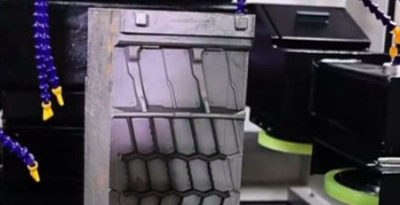
Cutting Methods for Crystalline Silicon Ingots
With the rapid development of clean energy, the goal of grid parity for photovoltaic power generation is also imminent. While various crystalline silicon manufacturers in the photovoltaic industry are continuously expanding their production capacity, they are also consistently reducing production costs, with the cutting of small silicon ingots being an important component of the cost of crystalline silicon solar cells.
- Crystalline silicon ingots can be cut with inner-diameter blades, slurry wire saws or fixed diamond wire loops; diamond wire is now the dominant method.
- Fixed-abrasive diamond wire produces a narrower kerf and a better surface than loose-abrasive slurry sawing, with no slurry to manage.
- Research and production data both show diamond wire loop cutting reduces kerf loss and raises yield for photovoltaic-grade silicon.
The methods below all feed into silicon wafer cutting, where kerf loss and TTV decide the final yield per ingot.
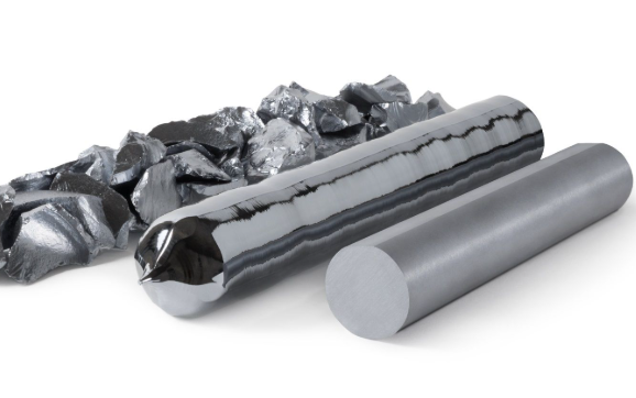

What is a silicon ingot?
A crystalline silicon ingot is a large, cylindrical (or quasi-square) monocrystalline or polycrystalline silicon rod with a regular atomic arrangement, produced by melting high-purity polysilicon raw material and employing precisely controlled crystal growth techniques. It serves as the direct precursor material for manufacturing silicon wafers.
Exceptionally High Purity: The silicon feedstock typically must achieve a purity level of at least 99.9999% (6N), while semiconductor-grade silicon requires up to 99.999999999% (11N). Such extremely low impurity content is essential for ensuring superior electrical properties.
Perfect Crystal Structure:
- Monocrystalline Silicon Ingots: The entire ingot exhibits a completely uniform atomic orientation with no grain boundaries. This structure delivers extremely high conversion efficiency and excellent electrical performance, making monocrystalline silicon the absolute mainstream material for high-efficiency solar cells and advanced semiconductor chips.
- Polycrystalline Silicon Ingots: Composed of numerous silicon grains of varying sizes separated by grain boundaries. While production costs are relatively lower, the conversion efficiency and electrical performance are slightly inferior to those of monocrystalline silicon.
Trend Toward Larger Dimensions: To enhance production efficiency and reduce downstream costs, the diameter of silicon ingots continues to increase. Currently, mainstream solar-grade monocrystalline silicon ingots have reached diameters of 210mm (G12) or larger, while semiconductor-grade ingots commonly correspond to wafer sizes of 200mm (8 inches) and 300mm (12 inc
Why diamond cutting wire loops are used for cutting crystalline silicon
In the process of cutting crystalline silicon ingots for solar energy applications, most manufacturers currently use traditional diamond saw blades along with steel wire and mortar for cutting. Diamond saw blades have fast cutting speeds but produce wide kerfs. During the cutting process, a large amount of silicon material is shaved into silicon powder that enters wastewater, resulting in high silicon losses.
The silicon consumption of diamond cutting wire loop cutting lines is one-third that of diamond saw blade cutting lines, allowing for significant silicon material savings. The cutting method using steel wire and mortar is slow, and both mortar and silicon powder enter wastewater together. The cost of separating them is high, with a considerable amount of mortar needing to be recovered, leading to adverse environmental impacts. Additionally, the cost of wastewater treatment is high.
The cutting speed of diamond cutting wire loops is 2-3 times faster than that of the mortar and steel wire cutting method, and the produced silicon powder is only mixed with water-based cooling liquid, resulting in lower wastewater treatment costs. By using diamond cutting wire loops for cutting crystalline silicon ingots, high-speed cutting, environmental friendliness, and low-cost production can be achieved.
The current development status of the diamond granite wire saw.
The electroplated diamond cutting wire has advantages such as strong cutting force and neat cutting seams in the cutting of crystalline silicon ingots, and has experienced rapid development in the past three years. It has not only been widely used in the photovoltaic industry but also in other fields such as sapphire and magnetic material cutting.
However, there are still issues in the production of electroplated diamond cutting wires, such as unstable processes, easy detachment of diamond particles, and high production costs, which hinder the widespread adoption of electroplated diamond cutting wires.
Research results on diamond wire loops.
Based on the fundamental theory of composite electroplating, this article investigates the process parameters affecting the electroplating of diamond cutting wire loops. In the experiments, a 0.27mm diameter copper-plated high carbon steel wire was used as the base wire. The electroplating solution employed a nickel sulfamate electroplating solution, and W30-40 diamond particles were used. Conclusions were drawn regarding the pre-treatment of diamond particles with nickel plating, with the chemical nickel plating method found to be most suitable for producing electroplated diamond cutting wire loops for cutting purposes. Through the study of different parameters of the weight ratio of nickel-plated diamond particles, a stable production weight ratio for nickel-plated diamond particles was determined.
By studying the impact of the current density of nickel electroplating with sulfamate on the brittleness of the coating, the optimal current density for producing electroplated diamond cutting wire loops was confirmed. Through investigating the effect of the thickness of sulfamate nickel electroplating on the cutting performance of electroplated diamond cutting wire loops, the optimal burial rate of diamond particles in the nickel plating layer was determined.
By studying the impact of the number of diamond particles per unit area on the cutting performance of electroplated diamond cutting wire loops, the optimal number of diamond particles per unit area corresponding to the best performance for cutting diamond wire loops for cutting was determined. Through investigating the effects of stress relief temperature and time on the cutting efficiency of electroplated diamond cutting wire loops, the optimal stress relief parameters were identified. Ultimately, industrial production of electroplated diamond cutting wire loops for cutting crystalline silicon ingots was achieved.
Frequently Asked Questions
What methods are used to cut crystalline silicon ingots?
The three historical methods are inner-diameter blade saws, loose-abrasive slurry wire saws and fixed diamond wire loops. Diamond wire loop cutting has become the mainstream choice.
Why is diamond wire loop preferred over slurry sawing?
Fixed diamond abrasive gives a narrower kerf, a cleaner process without slurry handling or disposal, and more wafers per ingot.
What is a crystalline silicon ingot?
It is a monocrystalline or multicrystalline silicon cylinder grown by methods such as Czochralski, which is then sliced into wafers for solar cells and semiconductor devices.
Technical content reviewed by the Ensoll engineering team — a diamond wire loop manufacturer with 10+ years of production experience.