The boom of silicon wafers in the photovoltaic industry
The boom of silicon wafers in the photovoltaic industry
- Carbon-neutrality goals worldwide have made photovoltaics the fastest-growing source of demand for silicon wafers.
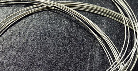
- PV wafer economics are driven by kerf loss and throughput, which is the main reason diamond wire replaced slurry saws across the industry.
- Larger wafer formats and thinner wafers are the PV industry’s structural cost-reduction path, and both raise the bar for cutting precision.
Under the background of the carbon neutralization goal and the accelerated application of global clean energy, China’s photovoltaic industry has achieved rapid growth as a whole.
According to industry standard announcements of enterprise information and industry associations, the main links of the national photovoltaic industry chain maintain a strong momentum of development, with a year-on-year growth rate of more than 45%.

Among them, polysilicon increased by 53.4% year-on-year, and silicon wafer increased by 45.5% year-on-year. Batteries increased by 46.6% year-on-year, and modules increased by 54.1% year-on-year. Overseas PV market demand continues to be strong, and both volume and price have risen.
In the first half of the year, the export volume of modules reached 78.6GW, a year-on-year increase of 74.3%, and the total export volume of photovoltaic products was about 25.9 billion US dollars, an increase of 113.1% year-on-year.
The iteration of photovoltaic technology has been accelerated, and the iteration of the technical route has prompted the update of a new generation of equipment to increase the value of the equipment.
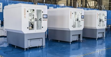
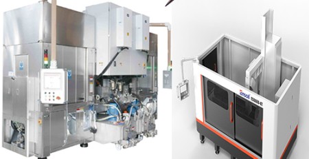
Silicon wafers are developing in the direction of large size, and silicon wafers are developing in the direction of thinning. Large-scale silicon wafer equipment will gradually usher in a large number of updates.
Cells will gradually develop in the direction of college cells, TOPCon and HJT will gradually become mainstream in the future, especially HJT will bring about the replacement of the entire production line equipment, resulting in a large space for equipment investment.
Crystalline silicon material is the most important photovoltaic material, with a market share of more than 90%. Solar-grade polysilicon for photovoltaic production requires a polysilicon purity of over 99.9999%.
According to the 2021 annual report on the external development of China’s photovoltaic industry, the national polysilicon production in 2021 will reach 505,000 tons, a year-on-year increase of 28.8%; the imported polysilicon is 2.04 billion US dollars, a sharp increase of 114% year-on-year, and the import volume is 114,000 tons, a year-on-year increase of 13.4% .
It is expected that there will still be a large capacity gap in upstream industrial silicon and polysilicon in the next five years. In addition, the new installed capacity of photovoltaics around the world is also growing steadily, driving the silicon industry chain to usher in a series of changes.
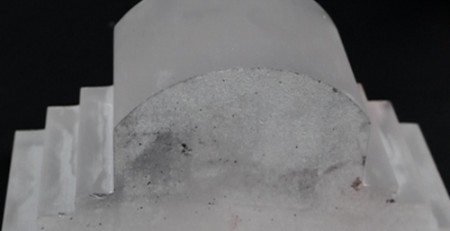
Photovoltaic silicon wafers are accelerating their development towards “large size” and “flakes”. As the area of the silicon wafer increases, the number of chips produced each time increases, and the probability of defects in the chip will also decrease, so the output of the chip will be significantly improved, thereby greatly reducing the cost.
Downstream silicon wafer companies continue to stimulate the demand for advanced production capacity expansion in large-scale competition, and old semiconductor factories are gradually being replaced.
How to produce qualified and larger-sized silicon wafers has always been a key concern of silicon wafer companies. Silicon wafer companies are also undergoing a new round of refresh.
In addition to the new capacity that silicon wafer manufacturers continue to expand, the replacement of stock capacity will also bring some equipment demand.
The PV wafer boom was not only a demand story — it was a wafer slicing cost story.
Frequently Asked Questions
Why is demand for silicon wafers booming?
Global carbon-neutrality targets are driving rapid photovoltaic installation growth, and every solar module starts as silicon wafers, so wafer demand scales directly with PV capacity.
What trends define photovoltaic wafer production?
Larger wafer formats, thinner wafers, diamond wire slicing and lower kerf loss are the main levers the industry uses to keep reducing cost per watt.
How does diamond wire cutting lower PV cost?
It produces more wafers per ingot with less silicon waste and cuts faster than slurry sawing, which reduces both material and process cost per watt.
Technical content reviewed by the Ensoll engineering team — a diamond wire loop manufacturer with 10+ years of production experience.