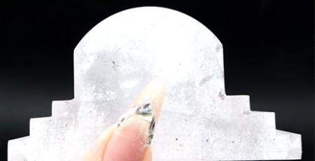
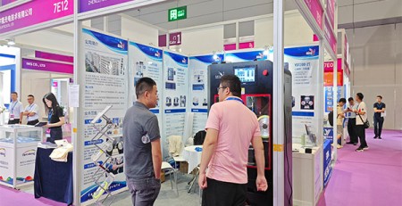
精密半导体切割解决方案
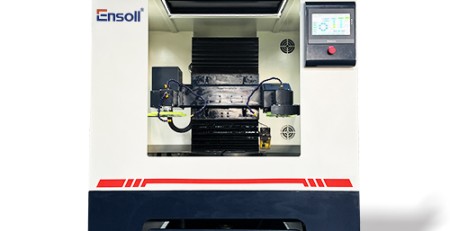
郑州, 中国 – 八月 5, 2025 – 元素工具 Technologies, 一种顶级的金刚石线锯切割解决方案供应商, has successfully completed precision cutting trials for semiconductor applications, further solidifying its partnerships with industry giants including TSMC and Samsung.
Cutting-Edge Semiconductor Solutions
During the demonstration at Ensoll’s advanced technology center, engineers showcased:
✔ Ultra-Precision Cutting
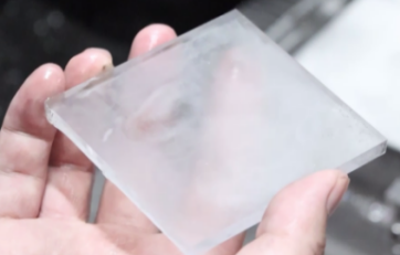
– Achieved micron-level accuracy (≤0.005mm TTV)
– Maintained exceptional surface quality (Ra <0.3微米)
✔ Full-Scale Production Capabilities
– From R&D prototyping to high-volume manufacturing
– Consistent performance across batch processing
✔ Industry-Proven Technology
– Optimized for semiconductor-grade materials
– Certified for cleanroom compatibility
Technical Specifications
| 参数 | Performance |
| 表面粗糙度 | Ra <0.3微米 |
| 线径 | 0.35-0.55毫米 |
| Production Capacity | 高达 500 cuts/hour |
为什么顶级半导体制造商选择Ensoll
1.全面支持
– 工艺开发协助
– 快速原型服务
– 生产规模指导
2.尖端创新
– 专有振动控制系统
– AI驱动的工艺优化
– 实时质量监控
客户推荐
“Ensoll的金刚石线切割技术使我们在半导体圆柱加工中实现了前所未有的精度,” 一位领先半导体制造商的高级工程师表示. “他们的解决方案已成为我们生产线的核心部分。”
关于Ensoll的半导体解决方案
我们的金刚石线锯切割系统提供:
– 等级 100 适合洁净室使用
– 自动化材料搬运选项
– 可定制各种晶圆尺寸
– 集成计量解决方案
新的合作伙伴发展
成功的试用已导致:
– Expansion of existing contracts with major foundries
– Joint development of next-generation cutting solutions
– Technical training programs for semiconductor engineers
Contact Our Semiconductor Experts