Der Boom der Siliziumwafer in der Photovoltaik-Industrie
Der Boom von Silizium-Wafer in the photovoltaic industry
- Carbon-neutrality goals worldwide have made photovoltaics the fastest-growing source of demand for silicon wafers.
- PV wafer economics are driven by kerf loss and throughput, was der Hauptgrund ist, warum Diamantdraht die Schlammsägen in der gesamten Branche ersetzte.
- Larger wafer formats and thinner wafers are the PV industry’s structural cost-reduction path, und beide erhöhen die Messlatte für Schnittpräzision.
Under the background of the carbon neutralization goal and the accelerated application of global clean energy, China’s photovoltaic industry has achieved rapid growth as a whole.
According to industry standard announcements of enterprise information and industry associations, the main links of the national photovoltaic industry chain maintain a strong momentum of development, mit einer jährlichen Wachstumsrate von mehr als 45%.

Darunter auch, Polysilizium ist gestiegen um 53.4% im Jahresvergleich, und Siliziumwafer sind gestiegen um 45.5% im Jahresvergleich. Batterien sind gestiegen um 46.6% im Jahresvergleich, und Module sind gestiegen um 54.1% im Jahresvergleich. Die Nachfrage auf dem ausländischen PV-Markt bleibt stark, und sowohl Menge als auch Preis sind gestiegen.
In der ersten Jahreshälfte, betrug das Exportvolumen von Modulen 78,6 GW, ein Anstieg im Jahresvergleich um 74.3%, und das gesamte Exportvolumen von Photovoltaikprodukten betrug etwa 25.9 Milliarden US-Dollar, eine Erhöhung von 113.1% im Jahresvergleich.
Die Weiterentwicklung der Photovoltaik-Technologie wurde beschleunigt, und die Weiterentwicklung der technischen Route hat die Aktualisierung einer neuen Generation von Anlagen zur Steigerung des Anlagenwertes veranlasst.
Siliziumwafer entwickeln sich in Richtung großer Größe, und Siliziumwafer entwickeln sich in Richtung Dünnung. Large-scale silicon wafer equipment will gradually usher in a large number of updates.
Cells will gradually develop in the direction of college cells, TOPCon and HJT will gradually become mainstream in the future, especially HJT will bring about the replacement of the entire production line equipment, resulting in a large space for equipment investment.
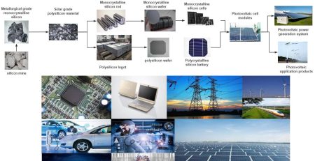
Crystalline silicon material is the most important photovoltaic material, with a market share of more than 90%. Solar-grade polysilicon for photovoltaic production requires a polysilicon purity of over 99.9999%.
According to the 2021 annual report on the external development of China’s photovoltaic industry, the national polysilicon production in 2021 will reach 505,000 Tonnen, ein Anstieg im Jahresvergleich um 28.8%; the imported polysilicon is 2.04 Milliarden US-Dollar, a sharp increase of 114% im Jahresvergleich, and the import volume is 114,000 Tonnen, ein Anstieg im Jahresvergleich um 13.4% .
It is expected that there will still be a large capacity gap in upstream industrial silicon and polysilicon in the next five years. Außerdem, the new installed capacity of photovoltaics around the world is also growing steadily, driving the silicon industry chain to usher in a series of changes.
Photovoltaic silicon wafers are accelerating their development towards “large size” und “flakes”. As the area of the silicon wafer increases, the number of chips produced each time increases, and the probability of defects in the chip will also decrease, so the output of the chip will be significantly improved, thereby greatly reducing the cost.
Downstream silicon wafer companies continue to stimulate the demand for advanced production capacity expansion in large-scale competition, und alte Halbleiterfabriken werden nach und nach ersetzt.
Wie man qualifizierte und größere Siliziumwafer herstellt, war schon immer ein zentrales Anliegen von Siliziumwafer-Unternehmen. Siliziumwafer-Unternehmen durchlaufen auch eine neue Runde der Erneuerung.
Neben der neuen Kapazität, die Siliziumwafer-Hersteller kontinuierlich ausbauen, wird auch der Ersatz von Bestandskapazitäten eine gewisse Nachfrage nach Ausrüstung mit sich bringen.
Der Boom der PV-Wafer war nicht nur eine Nachfragestory – es war auch eine Wafer-Schneidstory Kostenstory.
Häufig gestellte Fragen
Warum boomt die Nachfrage nach Siliziumwafern?
Globale Netto-Null-Ziele treiben das schnelle Wachstum der Photovoltaik-Installationen voran, und jedes Solarmodul beginnt als Siliziumwafer, daher skaliert die Wafer-Nachfrage direkt mit der PV-Kapazität.
Welche Trends kennzeichnen die Photovoltaik-Wafer-Produktion?
Größere Wafer-Formate, Dünnere Wafer, diamond wire slicing and lower kerf loss are the main levers the industry uses to keep reducing cost per watt.
How does diamond wire cutting lower PV cost?
It produces more wafers per ingot with less silicon waste and cuts faster than slurry sawing, which reduces both material and process cost per watt.
Technische Inhalte geprüft vom Ensoll-Engineering-Team – einem Hersteller von Diamantdraht-Schleifen 10+ Jahre der Produktionserfahrung.