En el mundo sofisticado de la fabricación de semiconductores, el viaje desde un lingote de silicio en bruto hasta un circuito integrado de alto rendimiento es una maravilla de la ingeniería moderna. Al principio de este viaje se encuentra un proceso que define la eficiencia de toda la cadena de suministro:Corte de obleas de silicio.
Mientras celebramos el 2026 Festival de los Faroles y esperamos un año de “Mejores” producción, Ensoll se enorgullece de liderar la vanguardia en soluciones de corte de alta precisión. Para los fabricantes, la elección de la herramienta de corte ya no es solo una decisión de adquisición, es un movimiento estratégico que dicta el rendimiento, costo, y la competitividad global.
1. El papel crítico del corte de obleas de silicio
El silicio sigue siendo la “base” de la era digital. Ya sea silicio monocristalino para CPUs de alta eficiencia o silicio policristalino para paneles solares, el objetivo del corte siempre es el mismo: producir obleas delgadas, planas, y sin daños con la menor pérdida de material.
El desafío de “El kerf”
En la industria de semiconductores, el silicio es esencialmente “oro líquido.” Cuando se corta un lingote, el grosor de la herramienta de corte crea un espacio llamado kerf. El material en este espacio se convierte en polvo fino (virutas) y se pierde para siempre. Traditional sawing methods often lose up to 30% Para 40% of the ingot to kerf loss.
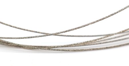
Ensoll’sSierra de hilo de diamantetechnology addresses this head-on. By utilizing ultra-thin wires (as thin as 80μm to 120μm), we minimize the “gap” and maximize the number of wafers harvested from a single ingot.
Presentación de videos: High-Speed Silicon Slicing
2. Why Diamond Wire Saw Outperforms Traditional Methods
For decades, the industry relied on Slurry Wire Saws (using loose silicon carbide grit in a liquid carrier). Sin embargo, as we move into 2026, DWS has become the undisputed champion. Aquí está la razón:
Un. Fixed Abrasive Efficiency
In a slurry saw, the grit “rolls” between the wire and the silicon, leading to a chaotic and slow cutting action. In an Ensoll Diamond Wire, the diamonds are electroplated directly onto the wire. Esta “fixed abrasive” method allows for:
Faster Linear Speeds: Reducing cutting time by up to 75%.
Lower Cutting Force: Minimizing the risk of wafer breakage.
B. Superior Surface Geometry
Semiconductor wafers must be perfectly flat. Any “bow” o “deformación” can cause errors during the subsequent lithography process. Ensoll’s wire saws provide:
Unmatched TTV (Variación del espesor total): Ensuring every wafer is uniform from edge to center.
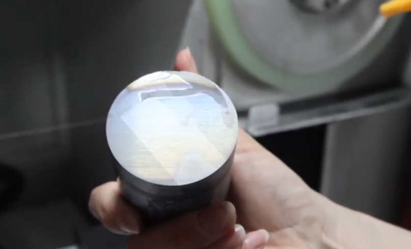
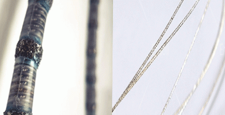
Reduced Saw Marks: A smoother surface means less time spent in the expensive Chemical Mechanical Polishing (CMP) stage.
Image Showcase: Comparación de calidad de superficie
3. The Technical Heart of Ensoll: Our Diamond Wire Construction.
Not all diamond wires are created equal. En Ensoll, our R&D has perfected a proprietary electroplating process that ensures the longevity and performance of our tools.
High-Tensile Core: We use premium high-carbon steel that can withstand the extreme tension required for high-speed wafering without snapping.
Diamond Grit Selection: We use synthetic diamonds with specific crystalline shapes to ensure maximum “bite” into the silicon.
Uniform Distribution: Nuestro “Mejores” 2026 manufacturing line ensures that diamond particles are distributed with mathematical precision, preventing “bald spots” on the wire that cause uneven cuts.
4. Expanding Beyond Silicon: SiC y GaN
The semiconductor landscape is shifting toward Wide Bandgap (WBG) materials like Silicon Carbide (Sic). These materials are nearly as hard as diamond itself, making them notoriously difficult to cut.
Ensoll’s diamond wire saw tools are specifically engineered for these “hard and brittle” challenges. By optimizing the bond between the diamond and the wire, we allow for the efficient slicing of SiC ingots, which is crucial for the burgeoning Electric Vehicle (VE) and 5G Power industries.
5. Environmental and Economic Impact: The Green Advantage
Sustainability is a core pillar of Ensoll’s 2026 mission. Traditional slurry sawing produces large amounts of toxic waste that is difficult to recycle.
Zero Slurry: DWS uses water-based coolants that are significantly easier to filter and recycle.
Energy Efficiency: Faster cutting times mean lower energy consumption per wafer.
Cost Reduction: By reducing kerf loss and polishing time, Ensoll helps manufacturers lower their Cost Per Wafer significantly.
6. Ensoll’s 2026 Service Guarantee: Our Three Promises
As highlighted in our Lantern Festival commencement, we are not just providing tools; we are providing a “Fullfillment” package:
Cumplimiento de Precisión: We guarantee that our wires will maintain consistent diameters throughout their lifespan, ensuring stable yields.
Cumplimiento del Servicio: Our Global 4-hour response team is active in every major tech hub (from Singapore to the UAE) to troubleshoot and optimize your lines.
Cumplimiento de la Asociación: We work with your engineers to customize wire specifications for your specific ingot sizes and machine types.
Silicon wafer cutting is the first cost-defining step in semiconductor fabrication: kerf loss directly sets how many wafers one ingot yields.
Diamond wire saw outperforms ID blades and slurry saws because fixed diamond abrasive gives a narrower kerf, better surface geometry and less material waste.
Ensoll diamond wire combines electroplated diamond grit with high-tensile steel wire, keeping tension stable and wire life long in production slicing.
La misma plataforma de hilo de diamante se extiende más allá del silicio a sustratos de SiC y GaN con velocidad ajustada, tensión y parámetros de refrigerante.
Conclusión: El “Mejores” Forma de cortar
La industria de los semiconductores se mueve a la velocidad de la luz, y su tecnología de corte debe mantenerse al día. El corte de obleas de silicio es la base sobre la cual se construye toda la tecnología moderna. Al asociarse con Ensoll y utilizar nuestras avanzadas soluciones de sierra de hilo de diamante, está eligiendo un camino de mayor eficiencia, lower waste, y precisión superior.
Mientras encendemos las linternas para 2026, dejemos que iluminemos el camino para su línea de producción. Experimente el “Cumplimiento de Precisión” que solo Ensoll puede proporcionar.
Preguntas Frecuentes
¿Por qué la sierra de hilo de diamante es el estándar para el corte de obleas de silicio??
El abrasivo de diamante fijo corta con un surco estrecho (típicamente 120-250 µm), mantiene firme el TTV y desperdicia mucho menos silicio que las cuchillas ID o el corte con lodo, so more wafers are produced per ingot.
What is kerf loss and why does it matter?
Kerf loss is the width of material removed by the cut. Every micrometer saved means more wafers per ingot, which is the dominant cost lever in silicon wafer production.
Can the same diamond wire saw cut SiC and GaN?
Sí. Diamond wire handles hard, brittle materials well; only process parameters such as wire speed, tension and coolant need to be adjusted for each material.
What surface quality does diamond wire cutting achieve?
As-cut surfaces typically reach Ra 0.2-0.5 µm with minimal sub-surface damage, which shortens downstream lapping and polishing time.
Contenido técnico revisado por el equipo de ingeniería de Ensoll — un fabricante de bucles de hilo de diamante con 10+ años de experiencia en producción.
Los ajustes para el corte en una sola dirección y el corte bidireccional son programas de corte específicos empleados por un solo alambre sierras de hilo diamantado... leer más
Ágata, con sus bandas hipnotizantes y colores vibrantes, es una piedra preciosa que ha cautivado a artesanos y coleccionistas durante siglos. Sin embargo,... leer más
Introducción a Soluciones Avanzadas de Corte de Vidrio
En el exigente panorama actual de la fabricación óptica, corte con sierra de hilo de diamante ha surgido como el estándar.... leer más
En el mundo de materiales avanzados, cortante carburo de silicio (Sic) presenta desafíos únicos que requieren soluciones especializadas. Como un.... leer más
Cuando la gente piensa en imanes potentes, neodimio (tierra rara) a menudo es lo primero que viene a la mente. Pero mucho antes de que el neodimio dominara el... leer más
Puntos clave
Un lazo de alambre de diamante es un bucle cerrado continuo de alambre de acero recubierto con abrasivo de diamante, corte de una sola vez.... leer más