En el mundo de la fabricación de precisión, Pocos procesos son tan críticos como cortar materiales duros en obleas delgadas, uniformes. Ya sea silicio para microchips, sustratos cerámicos para electrónica, o imanes de tierras raras para aplicaciones industriales, el proceso de corte de obleas es la columna vertebral de la microfabricación moderna.
El corte de obleas de silicio —también llamado aserrado de obleas de silicio o simplemente el proceso de corte de obleas— es el paso de producción que convierte un lingote monocristalino cultivado en los discos delgados utilizados para chips y células solares. Si estás preguntando cómo se cortan los obleas de silicio, la respuesta corta es un lazo de alambre de diamante que funciona a 10–25 m/s, donde el espesor de la oblea y la variación total del espesor (TTV) son determinados por la tensión del alambre y la velocidad de avance. La misma física rige el corte de obleas de silicio para fotovoltaicos y para sustratos de semiconductores; solo difieren el objetivo de espesor y la tolerancia al daño subsuperficial.
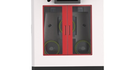
Pero el proceso de sierra de obleas no es un método único. Incluye técnicas como bucle de alambre de diamante cortante, corte con alambre EDM, e incluso máquinas compactas de mesa para R&D y producción en pequeños lotes.
Puntos clave
Un lazo de alambre de diamante corta silicio con un alambre de acero de 100–300 µm, electrochapado o unido con resina con polvo de diamante, funcionando a 10–25 m/s bajo refrigerante continuo.
Resultados típicos al cortar: 120– kerf de 250 µm, Acabado superficial Ra 0.2–0.5 µm, 2Velocidad de corte –10 mm/min.
El alambre de diamante reemplazó las sierras de hojas interiores y el corte con lodo principalmente debido a la pérdida de ranura: un corte más estrecho significa más obleas por lingote, que es la palanca de costo dominante en el silicio.
Los tres modos de defecto a controlar son rotura y desgaste del alambre, micro-grietas en la superficie, y curvatura del alambre causada por tensión desigual.
Corte de obleas de silicio, corte de obleas de silicio y el proceso de corte de obleas describen el mismo paso de producción: corte de obleas de silicio a partir de un lingote monocristalino con un alambre de diamante. Los objetivos de producción son típicamente una pérdida de ranura de 120–250 µm con TTV mantenido por debajo de 10 µm.
En esta guía, cubriré:
– Qué es una oblea (conceptos básicos de semiconductores)
– corte con alambre EDM como alternativa para materiales conductivos
– Table top cutter machines for laboratory and prototyping use
Let’s dive in:
1. What is a Wafer?
Before discussing how wafers are cut, we need to understand what a wafer actually is.
A wafer is a thin, flat disc of semiconductor material — most commonly silicon — on which microelectronic devices are built. Wafers serve as the substrate for integrated circuits (Ics), Células solares, LEDs, and MEMS (microelectromechanical systems).
– 12 Pulgadas (300milímetro) – industry standard today
– 18 Pulgadas (450milímetro) – emerging but rare
Thickness is typically between 500–800 microns, but after polishing and backgrinding, finished IC wafers can be as thin as 50–100 microns.
Why Precision Cutting Matters
A single wafer can yield thousands of individual chips (dies). Si el proceso de corte (troceado) es inexacto, pierdes chips, reduces el rendimiento, y aumentas los costos. Por eso el proceso de sierra de obleas debe ser extremadamente preciso — a menudo dentro de ±1–5 micrones.
2. Proceso de sierra de obleas (Bucle de alambre de diamante)
Ahora enfoquémonos en el núcleo de nuestro tema: el proceso de sierra de obleas usando un bucle de alambre de diamante.
Tradicional vs. Corte con Sierra de Diamante
Históricamente, las obleas se cortaban de lingotes usando discos de diámetro interno (ID) — sierras circulares con bordes impregnados de diamante. Pero los discos ID tienen limitaciones:
– Ranura ancha (pérdida de material)
– Velocidad de corte lenta
– Daño superficial
Entra el corte con hilo de diamante.
Cómo funciona el lazo de hilo de diamante
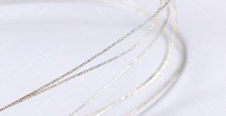
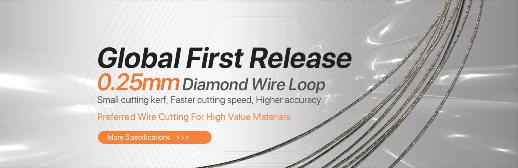
Un lazo de hilo de diamante consiste en un alambre de acero delgado (típicamente de 100–300 micrones de diámetro) electrodepositado o con resina unida con gránulos de diamante. El alambre se forma en un lazo continuo y se mueve mediante poleas a alta velocidad (10–25 m/s).
A medida que el cable se mueve, el diamante en polvo desgasta el material a través de un mecanismo de abrasión de tres cuerpos. Refrigerante (generalmente agua desionizada o fluido a base de aceite) elimina residuos y calor.
Principales Ventajas del Cable de Diamante para el Corte de Obleas
Criterio
Bucle de alambre de diamante
Corte por EDM con Hilo
Cortadora de Mesa (Alambre de diamante)
Tipo de material
No conductor & duro
Solo conductor
Igual que el cable de diamante
Ranura típica
120–250 µm
50–150 µm
150–300 µm
Acabado superficial
Bueno (Ra 0.2–0.5 µm)
Excelente (Ra 0.05–0.2 µm)
Bueno (Ra 0.3–0.6 µm)
Velocidad de corte
Rápida (2–10 mm/min)
Lento (0.5–3 mm/min)
Moderado (1–5 mm/min)
Costo del equipo
Alta (industrial) / Medio (de mesa)
Medio a alto
Bajo a medio
Mejor para
Obleas de silicio, cerámica, zafiro
Acero herramienta, carburo, titanio
R&D, pequeños lingotes, materiales frágiles
Proceso paso a paso para cortar obleas (Del lingote a la oblea)
1.Crecimiento de lingote – un lingote de silicio monocristalino se produce a través del método Czochralski o de la ZONA FLOTANTE.
Rectificado – el lingote se rectifica a un diámetro preciso.
Wire Sawing – Diamond wire loop slices the ingot into individual wafers.
Edge Rounding – Wafer edges are chamfered to prevent chipping.
Lapping – Removes saw marks and flattens the wafer.
Etching – Removes damaged surface layer.
Polishing – Creates mirror-like surface for lithography.
Applications Beyond Silicon
Diamond wire loop sawing isn’t only forobleas de silicio. It’s also used for:
– Carburo de silicio (Sic) – wide-bandgap semiconductor
– Arseniuro de galio (Gaas) – RF and LED applications
– Sapphire – for LED substrates and watch crystals
– Ceramic substrates – alumina, Zirconia
– Quartz and glass – optical and MEMS wafers
3. Corte por EDM con Hilo (A Complementary Technology)
While diamond wire sawing is excellent for non-conductive and hard materials, corte con alambre EDM (Mecanizado por descarga eléctrica) offers a completely different mechanism.
What is EDM Wire Cutting?
El corte por hilo EDM utiliza un hilo delgado, de latón o cobre eléctricamente cargado para erosionar materiales conductores a través de una serie de chispas eléctricas rápidas. El hilo nunca toca la pieza de trabajo — en su lugar, las chispas saltan a través de una pequeña distancia, fundiendo y vaporizando partículas diminutas.
Cómo Funciona
Electrodo de hilo (0.05– 3 mm de diámetro) se alimenta continuamente desde un carrete.
El agua desionizada actúa como un fluido dieléctrico, eliminando los residuos y controlando las chispas.
Los controles CNC mueven la pieza de trabajo en relación con el hilo.
Las chispas ocurren miles de veces por segundo, cortando gradualmente el metal.
Cuándo Usar Corte por Hilo EDM vs. Corte con Sierra de Diamante
Tipo de material
Método Recomendado
Silicio, cerámico, vidrio, zafiro
Bucle de alambre de diamante
Acero, carburo, titanio, Inconel
corte con alambre EDM
Materiales magnéticos (NdFeB, SmCo)
Ambos posibles; EDM evita el estrés mecánico
PCD (diamante policristalino)
EDM (el diamante es conductor si está dopado)
Ventajas del Corte por Hilo EDM
Sin contacto mecánico → no hay esfuerzo ni rebabas
Cuts extremely hard metals (HRC 60+)
Alta precisión (±1–2 microns)
Can cut complex 2D shapes (not just straight slices)
While EDM is rarely used to slice silicon ingots (silicon is only semi-conductive and EDM works poorly on high-resistivity Si), it is used for:
Cutting metalized ceramic substrates
Dicing copper-clad laminates
Slicing tungsten, molibdeno, or Kovar parts used in semiconductor
4. Table Top Cutter Machine
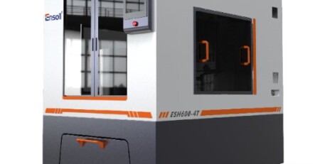
Not every wafer or material cutting job requires a massive industrial saw. For R&D labs, universities, small foundries, and prototype shops, a table top cutter machine is the perfect solution.
Typical Features
Compact footprint (fits on a lab bench)
Adjustable cutting speed and feed rate
Small cutting capacity (typically up to 50–100 mm diameter ingots or blocks)
Integrated coolant system (recirculating or gravity-fed)
Digital readout or CNC control (on high-end models)
Minimal waste – ideal for expensive materials like GaAs or SiC
1. Understanding Monocrystalline Silicon
Before diving into the cutting process, let’s briefly discuss monocrystalline silicon and why it requires specialized cutting techniques.
1.1 What isMonocrystalline Silicon? (You can also click the link to learn more details via Wikipedia.)
Monocrystalline silicon is a highly pure form of silicon with a single, continuous crystal lattice structure. It is produced using the Czochralski (CZ) method or the Float Zone (FZ) método, resulting in cylindrical ingots.
1.2 Por qué el corte de precisión es crítico
– Industria de semiconductores: Los obleas de silicio deben tener superficies ultra-lisas(rugosidad a nivel nanométrico) para la fabricación de microchips.
-Industria Fotovoltaica: Las células solares requieren delgadas, uniformes(típicamente 160-180µm) para maximizar la eficiencia.
– Pérdida mínima de corte: Reducir el desperdicio de material durante el corte mejora la eficiencia de costos.
Los métodos de corte tradicionales como sierras ID (sierras de diámetro interno) y sierras de múltiples hilos con lodo han sido reemplazadas por el corte con sierra de hilo de diamante debido a su rendimiento superior.
4. Desafíos & Soluciones en el corte con sierra de alambre de diamante
A pesar de sus ventajas, sierra de alambre de diamante enfrenta algunos desafíos:
4.1 Rotura del alambre & Desgaste
– Causa: Tensión excesiva, desgaste abrasivo, o falla del refrigerante.
– Solution: Monitoreo de tensión en tiempo real**, tamaño de grano de diamante optimizado, y filtración adecuada del refrigerante.
4.2 Microgrietas en la superficie
– Causa: Fractura frágil durante el corte.
– Solution: Tasa de alimentación controlada, grabado posterior al corte, o recocido.
4.3 Efecto de deformación del alambre
– Causa: Tensión desigual del alambre que genera cortes ondulados.
– Solution: Sistemas avanzados de guiado de alambre con control dinámico de tensión.
5.Aplicaciones del corte con sierra de alambre diamantado
5.1 Fotovoltaico (PV) Industria
– Producción de obleas solares (Mono PERC, TOPCon, Celdas HJT).
– Corte de obleas delgadas (menos de 150 µm para celdas de próxima generación de alta eficiencia).
5.2 Industria de semiconductores
– Corte de obleas de silicio para fabricación de circuitos integrados.
– Empaquetado avanzado** (p ej., empaquetado a nivel de oblea).
5.3 Otras aplicaciones
– Corte de sustratos de zafiro para LED.
– Mecanizado de materiales duros (Sic, cuarzo, cerámica).
6.Tendencias futuras en el corte de obleas de silicio
Obleas más delgadas: La demanda de obleas menores de 100 µm impulsa los avances en sierras de alambre diamantado de ultra-precisión.
IA & Automatización: Optimización de procesos basada en aprendizaje automático para mayor rendimiento.
Métodos de corte híbridos: Combinando pre-marcado con láser + sierra de alambre diamantado para obleas ultra-delgadas.
Conclusión
El proceso de sierra de obleas es una piedra angular de la fabricación moderna de electrónicos. Para materiales conductores en crecimiento, El corte con alambre EDM ofrece un método complementario sin contacto capaz de cortar aceros endurecidos, carburos, y superaleaciones con precisión a nivel de micrones.
Y para aquellos que trabajan en R&D, prototipado, o producción a pequeña escala, una máquina cortadora de mesa ofrece una opción asequible, punto de entrada flexible en el corte de alta precisión — sin el espacio en el piso o el presupuesto de una sierra de alambre industrial.
ya sea que esté fabricando obleas de silicio de 300 mm para procesadores de IA o cortando un pequeño sustrato de alúmina en un banco de laboratorio, comprender las fortalezas y limitaciones del lazo de alambre de diamante, EDM, y los cortadores de mesa le ayudará a seleccionar la herramienta adecuada para el trabajo. desde un lingote de silicio hasta cortarlo en cientos de obleas delgadas usando un lazo de alambre de diamante, cada paso requiere precisión, limpieza, y confiabilidad.
Preguntas Frecuentes
¿Cómo se cortan los obleas de silicio a partir de un lingote?
El lingote se cultiva mediante el método Czochralski o Float Zone, molido a un diámetro preciso, luego cortado con un lazo de alambre de diamante. Después del aserrado, los bordes de la oblea se biselan para prevenir astillado, y las obleas se lapean y pulen.
¿Qué es TTV en el corte de obleas?
TTV (variación total de espesor) es la diferencia entre los puntos más gruesos y más delgados de una oblea. Es la métrica principal para la calidad del aserrado de obleas porque la litografía posterior necesita una superficie plana, uniforme.
¿Por qué el alambre de diamante reemplazó al aserrado con lodo abrasivo?
El alambre de diamante fijo proporciona un canal más estrecho, un proceso más limpio sin abrasivo suelto que gestionar, y más obleas por lingote. El aserrado con lodo abrasivo desperdicia más silicio por corte y tiene mayores costos de consumibles y disposición.
¿Qué controla la rotura al cortar obleas más delgadas??
Monitoreo de tensión en tiempo real, grano de diamante del tamaño correcto, y refrigerante filtrado y limpio. A medida que los obleas disminuyen 150 µm, la estabilidad de la tensión y el control de alimentación importan más que la velocidad de corte.
¿Cuál es la diferencia entre el corte con hilo de diamante y el corte con hilo EDM para obleas??
El hilo de diamante corta materiales duros e no conductores con una ranura de 120–250 µm a 2–10 mm/min y Ra 0,2–0,5 µm. El corte con hilo EDM solo funciona en materiales conductores, es más lento a 0,5–3 mm/min, pero produce un acabado más fino de Ra 0,05–0,2 µm.
Qué diámetro de hilo se utiliza para el corte de obleas de silicio?
Típicamente hilo de núcleo de acero de 100–300 µm, que lleva grano de diamante en el rango de 30–100 µm, aplicado por electrodeposición o unión con resina. Un hilo más delgado reduce la pérdida de ranura pero requiere un control de tensión más estricto.
¿Qué tan delgadas pueden cortarse las obleas de silicio??
Las obleas solares de producción suelen tener 160–180 µm, Las celdas de próxima generación están bajando por debajo de eso 150 µm, Y las obleas de menos de 100 µm son el objetivo de desarrollo actual. Cada paso requiere un hilo más fino y un control de proceso más estricto.
¿Qué causa la curvatura del hilo?, ¿Y cómo se corrige??
La curvatura del hilo es un corte ondulado causado por una tensión desigual del hilo a lo largo del corte. Se corrige con sistemas avanzados de guía de hilo que aplican control dinámico de tensión durante todo el corte.
Contenido técnico revisado por el equipo de ingeniería de Ensoll — un fabricante de bucles de hilo de diamante con 10+ años de experiencia en producción.
En el mundo del corte industrial, La precisión y la eficiencia son primordiales. Una solución innovadora que ha ganado tracción recientemente.... leer más
Puntos clave
Las sierras de lazo de alambre de diamante cortan una gama excepcionalmente amplia de materiales compuestos metálicos y no metálicos, desde cerámica y vidrio... leer más
Puntos clave
Los mejores fabricantes de corte de materiales magnéticos combinan la tecnología de sierras de alambre de diamante, tolerancias estrictas y cero daño térmico — el... leer más
Una sierra de alambre de diamante sin fin Ensoll ESO-GM cortó muestras de tubos metálicos de clientes europeos en 3 secciones de mm con TTV ≤.... leer más
Introducción: Revolutionizing Optical Crystal Processing
In the precision-driven world of optical manufacturing, la calidad del corte del cristal impacta directamente en el rendimiento... leer más
Puntos clave
Los tubos de acero elástico son duros y resistentes, por lo tanto, la selección del método de corte tiene un gran impacto en la calidad del corte, rebaba... leer más
Puntos clave
El corte de obleas de semiconductores es un paso crítico en la fabricación de CI donde la precisión y la integridad de la superficie determinan el rendimiento del dispositivo.
Un corte con diamante.... leer más
Ágata, con sus bandas hipnotizantes y colores vibrantes, es una piedra preciosa que ha cautivado a artesanos y coleccionistas durante siglos. Sin embargo,... leer más
Abstracto: Este informe de aplicación documenta una prueba de corte en rebanadas rectas de precisión en PMI
(polimetacrilimida) espuma estructural suministrada por un cliente europeo. Cuatro rebanadas... leer más

 Typical Wafer Sizes
 What is EDM Wire Cutting?
 Monocrystalline silicon is a highly pure form of silicon with a single, continuous crystal lattice structure. It is produced using the Czochralski (CZ) method or the Float Zone (FZ) método, resulting in cylindrical ingots.