How to process silicon carbide?
How to process silicon carbide?
Silicon carbide (SiC) material is the main development direction of the power semiconductor industry. It is used to make power devices and can significantly improve the utilization rate of electric energy. In the foreseeable future, new energy vehicles will be the main application scenario of silicon carbide power devices.
As a technology pioneer, Tesla has taken the lead in integrating full silicon carbide modules in Model 3, and other first-tier car companies are also planning to expand the application of silicon carbide. With the decreasing manufacturing cost of silicon carbide devices and the gradual maturity of process technology, the future of the silicon carbide power device industry is promising.

What is Silicon Carbide?
Silicon carbide (SiC) is a third generation compound semiconductor material. The cornerstone of the semiconductor industry is chips. The core materials for making chips are divided into:
The first generation of semiconductor materials (mostly high-purity silicon that is widely used at present), the second generation of compound semiconductor materials (gallium arsenide, indium phosphide), third-generation compound semiconductor materials (silicon carbide, gallium nitride).
Because of its superior physical properties: high band gap (corresponding to high breakdown electric field and high power density), high electrical conductivity, and high thermal conductivity, silicon carbide will be the most widely used basic material for making semiconductor chips in the future.
The main form of silicon carbide in semiconductor chips is the substrate. Semiconductor chips are divided into integrated circuits and discrete devices, but whether it is an integrated circuit or a discrete device, its basic structure can be divided into a “substrate-epitaxial-device” structure. The main form of silicon carbide in semiconductors is as a substrate material.
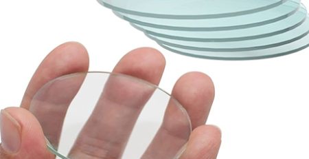
Silicon carbide wafer is a single crystal thin slice formed by cutting, grinding, polishing, cleaning and other processes of silicon carbide crystal. As a semiconductor substrate material, silicon carbide wafers can be made into silicon carbide-based power devices and microwave radio frequency devices through epitaxial growth, device manufacturing and other links, and are an important basic material for the development of the third-generation semiconductor industry.
According to different resistivity, silicon carbide wafers can be divided into conductive type and semi-insulating type. Among them, conductive silicon carbide wafers are mainly used in the manufacture of high-temperature and high-voltage power devices, with a large market size; semi-insulating silicon carbide substrates are mainly used in microwave radio frequency devices and other fields.
With the accelerated construction of 5G communication networks, The market demand has increased significantly.The hardness of SiC is second only to diamond. It not only has the characteristics of high hardness, but also has high brittleness and low fracture toughness.
Silicon carbide processing process
Silicon carbide wafers use high-purity silicon powder and high-purity carbon powder as raw materials, and use physical vapor transport (PVT) to grow silicon carbide crystals and process them into silicon carbide wafers.
① Raw material synthesis. The high-purity silicon powder and high-purity carbon powder are mixed in a certain proportion, and the silicon carbide particles are synthesized by reaction at a high temperature above 2,000 °C. After crushing, cleaning and other processes, high-purity silicon carbide micropowder raw materials that meet the requirements of crystal growth are obtained.
② crystal growth. Using high-purity silicon carbide micropowder as raw material, using the self-developed crystal growth furnace, the silicon carbide crystal is grown by the physical vapor transport method (PVT method).
The high-purity silicon carbide powder and the seed crystal were placed at the bottom and top of the cylindrically sealed graphite crucible in the single crystal growth furnace, respectively.
The crucible is heated to above 2,000°C by electromagnetic induction, and the temperature at the seed crystal is controlled to be slightly lower than that at the lower part of the micropowder, forming an axial temperature gradient in the crucible.
The silicon carbide micropowder sublimates at high temperature to form Si2C, SiC2, Si and other substances in the gas phase, and is driven by a temperature gradient to reach the seed crystal with a lower temperature, and crystallizes on it to form a cylindrical silicon carbide ingot.
③Ingot processing. The prepared silicon carbide ingot is oriented using an X-ray single crystal orientation instrument, and then ground, rolled, and cropping silicon carbide crystals of standard diameter size. The latest process for cropping of silicon carbide crystals uses a diamond wire loop saw for cropping.
④Crystal cutting. Using multi-wire cutting equipment, the silicon carbide crystals are cut into thin slices up to 1mm thick.
⑤Wafer grinding. The wafers are ground to the desired flatness and roughness through diamond slurry of different particle sizes.
⑥ Wafer polishing. The silicon carbide polishing sheet with no damage on the surface is obtained by mechanical polishing and chemical mechanical polishing.
⑦ Wafer detection.
Using optical microscope, X-ray diffractometer, atomic force microscope, non-contact resistivity tester, surface flatness tester, surface defect comprehensive tester and other equipment, detect the microtube density, crystal quality, surface roughness, resistivity, warpage, curvature, thickness change, surface scratches and other parameters of the silicon carbide wafer, and determine the quality level of the wafer accordingly.
⑧ Wafer cleaning. The silicon carbide polishing sheet is cleaned with cleaning agent and pure water to remove surface contaminants such as polishing liquid remaining on the polishing sheet, and then the wafer is blown and dried by ultra-high-purity nitrogen and a drying machine; The clean room is packaged in a clean wafer cassette to form a silicon carbide wafer ready for downstream use.
The larger the wafer size, the more difficult it is to grow and process the corresponding crystal, and the higher the manufacturing efficiency of downstream devices and the lower the unit cost. At present, international silicon carbide wafer manufacturers mainly provide 4-inch to 6-inch silicon carbide wafers, and international leading companies such as CREE and II-VI have begun to invest in the construction of 8-inch silicon carbide wafer production lines.