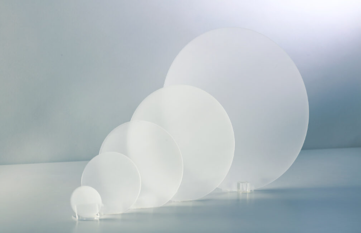
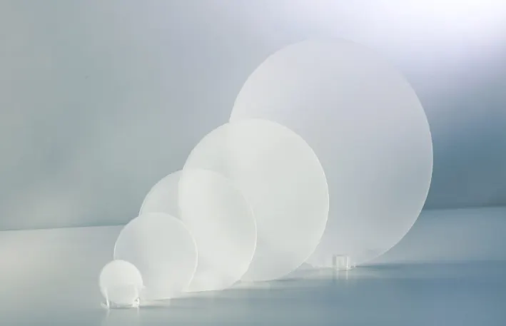
Sapphire substrates are critical components in LED manufacturing, optical devices, and semiconductor applications. しかし, cutting sapphire—a material with a Mohs hardness of 9—poses significant challenges. Traditional methods like blade sawing or laser cutting often lead to cracks, high material loss, and uneven surfaces.
重要なポイント
サファイア (Mohs 9) is both extremely hard and brittle: blade sawing and laser cutting often cause cracks, uneven surfaces, and up to 30% material loss.
A diamond wire loop can be as thin as 0.1 mm versus a 0.3 mm or wider blade kerf, so more wafers are recovered from every crystal ingot.
The low-force wire cut generates far less mechanical stress, preventing subsurface micro-cracks and leaving a smoother surface that needs less polishing.
Modern machines cut sapphire at 0.5-2 ミリメートル/分, and multi-wire systems can slice hundreds of wafers simultaneously.
Main beneficiaries: LED sapphire substrates, ultra-thin semiconductor wafers (down to about 100 micrometers), and optical windows and lenses.
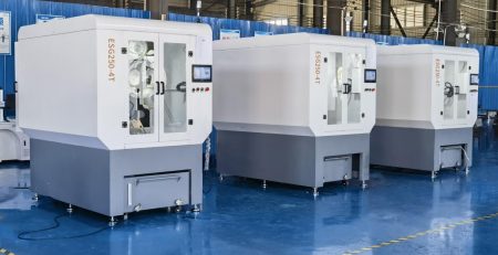
ダイヤモンドワイヤーループcutting has emerged as the superior solution, offering higher precision, minimal kerf loss, and reduced subsurface damage. この記事の内容, we explore how this advanced technology improves efficiency in sapphire substrate production.
Challenges in Sapphire Substrate Cutting
Before discussing diamond wire loops, it’s essential to understand the difficulties in processing sapphire:
Extreme Hardness – Sapphire is one of the hardest materials, making mechanical cutting difficult.
Brittleness – Improper cutting can cause micro-cracks, reducing substrate quality.
High Precision Requirements – LED and semiconductor industries demand ultra-thin wafers (as low as 100µm) with near-perfect surfaces.
Material Waste – Conventional methods lose up to 30% of the material, increasing costs.
Traditional methods like ID saws (inner diameter saws) and laser cutting struggle with these challenges, leading to higher rejection rates and production inefficiencies.
How Diamond Wire Loop Cutting Works
Diamond wire loop technology uses a thin, flexible wire embedded with diamond particles to slice through sapphire with minimal force. Here’s how it enhances efficiency:
1.Precision Cutting with Minimal Kerf Loss
– The wire diameter can be as thin as 0.1mm, significantly reducing material waste compared to blade saws (which have a kerf of 0.3mm or more).
– This allows more wafers per crystal ingot, lowering production costs.
– The result is a smoother surface finish, reducing the need for extensive polishing.
3.Faster Cutting Speeds
– 高度な ダイヤモンドワイヤーループmachines can achieve cutting speeds of 0.5–2 mm/min, much faster than traditional methods.
– Multi-wire systems can cut hundreds of wafers simultaneously, boosting productivity.
4.Lower Operating Costs
– Diamond wire loops have a longer lifespan than abrasive blades, reducing replacement frequency.
– Less coolant is required compared to traditional sawing, lowering environmental and operational costs.
Applications in the LED and Semiconductor Industry
The benefits ofダイヤモンドワイヤーループcutting make it ideal for:
✅ LED Manufacturing – Producing high-quality sapphire substrates for brighter, more efficient LEDs.
✅ Semiconductor Wafers – Enabling ultra-thin wafers for advanced electronics.
✅ Optical Components – Cutting sapphire windows and lenses with superior surface integrity.
結論
Diamond wire loop cutting has revolutionized sapphire substrate processing by improving precision, reducing waste, and increasing production efficiency. As demand for high-performance LEDs and semiconductors grows, this technology will remain a critical tool for manufacturers seeking cost-effective, high-quality solutions.
Interested in optimizing yoursapphire cutting process? Contact us today to learn how diamond wire loops can enhance your production line!
よくある質問
Why is sapphire so difficult to cut?
Sapphire rates 9 on the Mohs hardness scale and is highly brittle, so conventional blade or laser cutting easily produces micro-cracks and high rejection rates. The LED and semiconductor industries also demand ultra-thin wafers with near-perfect surfaces, which leaves almost no margin for error.
How does a diamond wire loop reduce sapphire material waste?
The wire can be as thin as 0.1 ミリメートル, compared with a blade kerf of 0.3 mm or more. Conventional methods lose up to 30% of the ingot, while the narrow wire kerf converts more of each crystal into usable wafers and lowers production cost.
Does diamond wire loop cutting damage the sapphire surface?
いいえ. Because the wire cuts with very low force, it generates less mechanical stress than abrasive saws, which prevents subsurface micro-cracks. The resulting surface is smoother and requires less polishing afterward.
Which industries use diamond-wire-cut sapphire substrates?
LED manufacturing uses them for brighter, more efficient chips; the semiconductor industry uses ultra-thin sapphire wafers for advanced electronics; and optics producers cut sapphire windows and lenses with superior surface integrity.
Silicon carbide wafer application and future development trend
Key Takeaways
Silicon carbide is the main development direction of the power semiconductor industry.
SiC.... 続きを読む
Classification of new functional ceramic materials
New functionalセラミックmaterials are dielectric materials with electrical, マグネチック, オプティカル, アコースティック, 熱の, メカニカル,... 続きを読む
Traditional solar cell production process
Key Takeaways
Traditional solar cell production starts with silicon wafer manufacturing and proceeds through texturing, 拡散, エッチング,... 続きを読む
Types of Optical Glass
Key Takeaways
Optical glass comes in six main types: colorless optical glass, anti-radiation optical glass, radiation-resistant optical glass,... 続きを読む
Key Takeaways
Industrial ceramics are fine ceramics used in industrial production, delivering mechanical, thermal and chemical functions in application.
High temperature, corrosion,... 続きを読む