Semiconductor Crystal Cutting with Diamond Wire Loop
- Semiconductor crystal cutting transforms raw ingots into wafers, and the slicing step sets both yield and downstream surface quality.
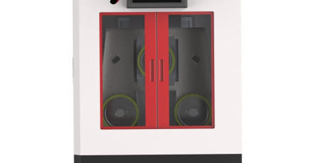
- Diamond wire loop cutting works by running a diamond-coated wire at high speed under coolant, grinding the crystal with a narrow, controlled kerf.
- Compared with ID blades and slurry saws, diamond wire loop cuts Si, SiC, GaN and sapphire with less material loss and lower sub-surface damage.
Introduction to Semiconductor Crystal Cutting
The semiconductor industry relies on precision cutting technologies to transform raw crystal ingots into functional wafers for electronic devices. Among various cutting methods, diamond wire loop technology has emerged as the gold standard for processing advanced semiconductor materials. This innovative approach offers unparalleled precision when working with challenging materials like Silicon Carbide (SiC) and Gallium Nitride (GaN), while maintaining efficiency for traditional silicon wafers.
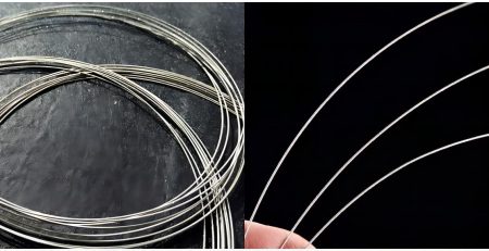
Diamond wire loop cutting utilizes a thin, flexible wire embedded with diamond particles to achieve clean, precise cuts through even the hardest semiconductor crystals. The technology has revolutionized wafer production by significantly reducing material loss and improving surface quality compared to conventional blade-based methods. As semiconductor devices continue to shrink in size while demanding higher performance, the precision offered by diamond wire cutting becomes increasingly critical.
The Diamond Wire Loop Cutting Process
How Diamond Wire Loop Technology Works
The diamond wire loop system consists of a continuous wire coated with industrial diamond particles running through a series of precision guides. During operation:
- The wire moves at controlled speeds (typically 10-30 m/s)
- Tension is maintained at optimal levels (usually 15-30 N)
- Cutting fluid is applied to reduce heat and remove debris
- Computer-controlled positioning ensures accurate cuts
This configuration allows for:
→ Uniform material removal
→ Minimal kerf loss
→ Excellent surface finish
→ Reduced subsurface damage
Advantages Over Traditional Cutting Methods
Compared to conventional inner diameter (ID) saws or laser cutting:
- Material Savings: Kerf loss reduced by 50-70%
- Quality Improvement: Surface roughness improved by 30-50%
- Versatility: Capable of cutting ultra-hard materials like SiC
- Productivity: Multi-wire systems can cut hundreds of wafers simultaneously
- Cost Efficiency: Longer tool life and lower energy consumption
Cutting Different Semiconductor Materials
Silicon Wafer Cutting (Monocrystalline & Polycrystalline)
Silicon remains the workhorse of semiconductor manufacturing, with both monocrystalline and polycrystalline varieties requiring precise cutting:
Monocrystalline Silicon:
- Preferred for high-performance ICs and solar cells
- Diamond wire parameters:
– Wire diameter: 0.12-0.18 mm
– Diamond grit size: 15-25 μm
– Cutting speed: 0.5-1.5 mm/min
Polycrystalline Silicon:
- Used for cost-sensitive applications like solar panels
- Cutting considerations:
– Slightly larger diamond grit (20-30 μm)
– Higher feed rates possible
– Less sensitivity to crystal orientation
Silicon Carbide (SiC) Processing Challenges
 SiC presents unique cutting difficulties due to:
- Extreme hardness (Mohs 9.5, nearly as hard as diamond)
- High brittleness
- Costly raw materials (making material conservation critical)
Diamond wire loop solutions for SiC:
- Specialized diamond bonding for improved particle retention
- Optimized coolant formulations
- Advanced tension control systems
- Typical cutting speeds: 0.3-0.8 mm/min
Compound Semiconductors: GaAs, InP, and GaN
Gallium Arsenide (GaAs):
- Used for RF and optoelectronic devices
- Cutting requirements:
– Low tension to prevent cracking
– Alcohol-based coolants
– Medium diamond grit sizes (20-30 μm)
Indium Phosphide (InP):
- Critical for photonic applications
- Processing considerations:
– Very low mechanical stress cutting
– Temperature-controlled environments
– Ultra-fine diamond particles (10-15 μm)
Gallium Nitride (GaN):
- Enabling next-gen power electronics
- Cutting parameters:
– Moderate tension settings
– Diamond-coated wire with nickel matrix
– Cutting speeds similar to SiC
Optimizing Diamond Wire Loop Performance
Key Process Parameters
To achieve optimal cutting results, manufacturers must carefully control:
- Wire Specifications
– Diameter (typically 0.1-0.2 mm)
– Diamond particle size (10-30 μm)
– Bonding matrix composition
- Operating Conditions
– Wire speed (10-30 m/s)
– Tension force (15-30 N)
– Feed rate (material-dependent)
– Coolant flow and composition
- Machine Configuration
– Guidance system precision
– Vibration isolation
– Automation features
Quality Control Measures
Implementing robust QC protocols ensures consistent results:
- Pre-cut material inspection
- Real-time process monitoring
- Post-cut wafer characterization
– Surface roughness measurements
– Thickness variation analysis
– Subsurface damage evaluation
- Statistical process control implementation
Industry Applications and Case Studies
Solar Photovoltaic Manufacturing
iamond wire cutting has transformed solar cell production:
- 40% reduction in silicon waste
- 30% increase in cutting throughput
- Improved wafer strength for thinner designs
- Case study: Leading PV manufacturer increased yield by 22% after switching to diamond wire
Power Electronics Production
SiC and GaN device manufacturing benefits include:
- Cleaner edges for improved device performance
- Ability to process larger diameter wafers
- Reduced breakage during handling
- Example: EV inverter producer reduced defect rates by 35%
RF and Optoelectronic Components
Precision cutting of GaAs and InP enables:
- Higher frequency device performance
- Improved photonic device efficiency
- Better yield for expensive compound materials
- Application: 5G RF filter manufacturer achieved 15% cost reduction
Future Trends in Diamond Wire Cutting
Technology Advancements
Emerging innovations include:
- Smart wires with embedded sensors
- AI-driven process optimization
- Nanocomposite diamond coatings
- Dry cutting developments for certain applications
Market Growth Projections
The diamond wire cutting market for semiconductors is expected to:
- Grow at 12.5% CAGR through 2030
- Reach $1.2 billion by 2028
- Expand into new materials like Ga₂O₃
Conclusion and Implementation Guide
Diamond wire loop cutting has become indispensable for modern semiconductor manufacturing. When implementing this technology:
- Material Assessment
– Evaluate crystal properties
– Determine quality requirements
– Calculate ROI potential
- System Selection
– Choose appropriate wire specifications
– Select machine capabilities
– Consider automation needs
- Process Development
– Optimize cutting parameters
– Establish QC protocols
– Train operators
- Continuous Improvement
– Monitor performance metrics
– Implement upgrades
– Stay current with technology trends
For semiconductor manufacturers looking to improve yields, reduce costs, and enhance product quality, diamond wire loop cutting offers a proven solution that continues to evolve with the industry’s needs.
Crystal orientation and feed rate matter here for the same reasons they do in cutting silicon wafers, where chipping directly reduces usable area.
Frequently Asked Questions
How does diamond wire loop cutting work for semiconductor crystals?
A closed loop of steel wire coated with diamond abrasive runs continuously at high speed under coolant, micro-grinding the crystal into wafers with a narrow, well-controlled kerf.
What are the advantages of diamond wire loop over traditional cutting methods?
Narrower kerf loss, better surface geometry, no slurry to manage, and far less sub-surface damage than ID blade or slurry sawing.
Can diamond wire loop cut SiC, GaN and sapphire as well as silicon?
Yes. Diamond is the hardest abrasive, so the same platform cuts all common semiconductor crystals; only speed, tension and coolant parameters are adjusted per material.
Technical content reviewed by the Ensoll engineering team — a diamond wire loop manufacturer with 10+ years of production experience.