Резка карбида кремния: Руководство по алмазной проволочной пиле
В требовательном мире передовых полупроводников, где производительность и эффективность имеют первостепенное значение, один материал является критическим фактором: Карбид кремния (Так). Known for its exceptional hardness (второй по твердости после алмаза), высокая теплопроводность, and superior electrical properties, SiC is the cornerstone of next-generation power electronics. Однако, its very advantages make it notoriously difficult to process. This is where the transformative power of the Алмазная канатная пила comes into play, acting as the scalpel that unlocks the potential of this super material.
- Silicon carbide ranks about 9.2–9.5 on the Mohs scale — close to diamond — and combines that hardness with brittleness, so blade and laser cutting both leave damage.
- Diamond wire is the matching tool: it cuts SiC cold with a continuous abrasive action instead of impact or heat, which avoids the micro-cracking that ruins SiC wafers.
- Blade dicing typically leaves more than 20 µm of edge chipping on SiC. Diamond wire holds chipping to near zero, and that difference is what protects yield on power devices and RF chips.
- In production, switching from laser to diamond wire on SiC MOSFET cutting lifted yield from 78% Кому 93% at 500 mm/min — the gain came almost entirely from eliminating crack-induced failures.
- Wire can run as fine as 0.2 миллиметр. Because SiC boules are expensive, that narrow kerf converts directly into more wafers per crystal.
- For SiC/GaN work, specify wire 0.1–0.3 mm in diameter with 10–20 µm diamond grit, and hold machine vibration below 0.1 µm — grit cuts the material, but vibration is what creates the micro-cracks.
- GaN fails differently from SiC: it is less hard but has high fracture toughness, so it cracks rather than abrades. Low-vibration wire cutting matters more on GaN than raw abrasive hardness.
The SiC Challenge: Материал, трудный для обработки
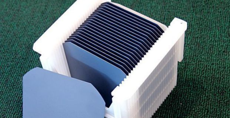
Прежде чем SiC сможет стать сердцем эффективного инвертора для электромобиля или компактного преобразователя для энергосети, его необходимо точно нарезать из цельного булла на тонкие пластины. Традиционные методы резки, например, абразивные распилочные станки со шлифовальной суспензией, испытывают трудности с SiC. Они медленные, создают значительные отходы, и, и, что наиболее критично, вызывают микротрещины под поверхностью и высокий уровень напряжений в хрупком кристалле. Эти дефекты становятся причиной снижения производительности, уменьшая выход и надежность конечных чипов. Отрасли было необходимо решение, которое соответствовало бы твердости SiC с равной точностью и деликатностью.
 Почему алмазная проволочная пила идеально подходит для SiC
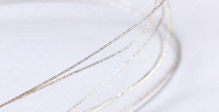
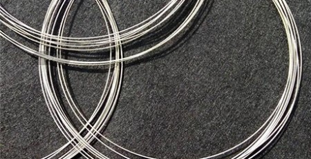
Алмазная проволочная пила работает по элегантно простому, но глубоко эффективному принципу: непрерывная петля стальной проволоки, покрытой толстым слоем алмазных частиц, moves at high speed to perform a clean, linear cut. For SiC, this technology offers a suite of unbeatable advantages:
- Минимальные потери при резе, Maximized Yield: The diamond wire can be incredibly thin (as fine as 0.2mm). This creates an extremely narrow cut path, or “kerf.” Given the high cost of SiC boules, every millimeter saved translates directly into more wafers per crystal and substantial material cost savings. This efficiency is fundamental for making SiC technology more commercially viable.
- Superior Surface Integrity: Непрерывное, controlled cutting action of the wire generates minimal mechanical and thermal stress. The result is a wafer surface with exceptional as-cut quality—smoother and with dramatically fewer micro-cracks compared to traditional methods. This “low-damage” surface means the subsequent, затраты времени на шлифовку и полировку могут быть значительно снижены, ускорение всего производственного процесса.
- Нескомпромиссное качество кристалла: Возможно, самым критическим преимуществом для полупроводниковых применений является сохранение присущих электрических свойств SiC. Чистый, низконапряженный рез гарантирует, что кристаллическая решетка на краю и поверхности пластины остается неповрежденной. Это напрямую способствует более высокой производительности чипов, лучшим характеристикам пробойного напряжения, и в конечном итоге, более надежным и мощным электронным устройствам.
- Охлаждаемая и контролируемая обработка: Рез обычно выполняется с использованием водосодержащей охлаждающей жидкости, что предотвращает локальный перегрев, который может изменить свойства материала. This “холодная резка” процесс необходим для поддержания точного стехиометрического состава и качества, требуемого для полупроводников высокого уровня.
From Wafer to Wonder: The Journey of a Cut SiC Wafer
Once sliced and polished, these pristine SiC wafers become the foundation for a technological revolution. Their primary destination is the fabrication of power semiconductor devices
- Electric Vehicles (Электромобили): SiC MOSFETs and diodes form the core of the main traction inverter. They switch electricity with far less loss than traditional silicon chips, enabling longer driving range, faster charging, and more compact, efficient powertrains.
- Renewable Energy: In solar inverters and wind turbine converters, SiC devices handle high voltages and frequencies with exceptional efficiency, minimizing energy loss as green power is fed into the grid.
- 5G & RF Infrastructure: Высокочастотные возможности карбида кремния делают его идеальным для силовых радиочастотных усилителей в следующем поколении базовых станций связи, обеспечивая более быструю передачу данных.
- Промышленные приводные двигатели: Приводы на основе карбида кремния позволяют создавать более компактные, и более эффективные системы управления промышленными двигателями, что приводит к значительной экономии энергии в производстве и автоматизации.
Понимание твердости и характеристик алмазной канатной пилы
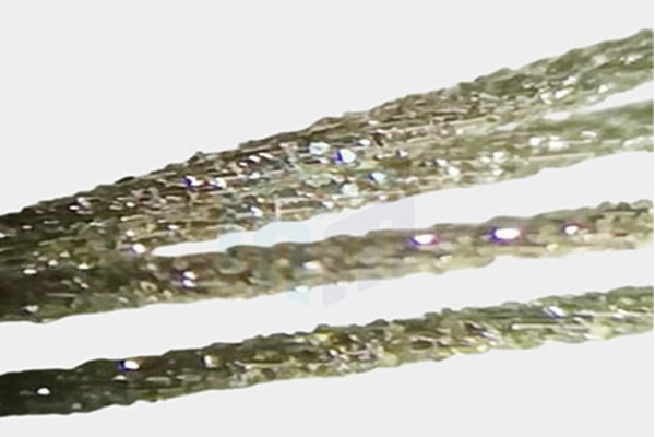
- Твердость алмазных канатных пил обусловлена частицами алмаза, встроенными в проволоку. Алмазы известны своей исключительной твердостью, Считается самым твердым материалом природного происхождения. При встраивании в канатную пилу, Алмазы обеспечивают превосходную режущую кромку, которая может легко проникать и шлифовать различные материалы.

Понимание твердости и характеристик карбида кремния
Проблемы при резке карбида кремния
1. Чрезвычайная твердость и хрупкость:
С твердостью по шкале Мооса примерно 9.5, только немного уступая алмазу и нитриду бора, карбид кремния является чрезвычайно твердым и хрупким материалом. Обычные режущие инструменты быстро изнашиваются, что приводит к низкой экономической эффективности. Еще более критично, хрупкость делает его очень склонным к образованию микротрещин, сколы на краях, и повреждений под поверхностью при механической резке. Этот повреждённый слой может значительно ухудшить производительность и надёжность конечного полупроводникового устройства.
Последний обзор: Сентябрь 2026
2. Низкая эффективность резки и высокий износ инструмента:
Использование алмазных инструментов (таких как алмазная проволока или диски) почти обязательно. Однако, даже алмазные абразивы испытывают значительный износ при резке SiC, что приводит к снижению скорости резки со временем, увеличению тепловыделения, и высоким расходам на материалы. Процесс часто требует нескольких этапов (черновой и окончательной обработки) чтобы достичь требуемой целостности поверхности, дополнительно снижая общую производительность.
3. Требования к ультравысокой точности и качеству поверхности:
Полупроводниковые пластины требуют исключительной геометрической точности (плоскостности и однородности толщины на нанометровом уровне) и поверхности без повреждений, с ультрачистой поверхностью. Любые микро-трещины или внутренние напряжения, возникающие при резке, должны быть сведены к минимуму, так как повреждения могут распространяться на последующих этапах шлифовки и полировки, вызывая поломку подложек или брак компонентов. Достижение этого при одновременном поддержании высокого выхода является одной из основных проблем.
4. Тепловое управление и контроль напряжений:
Процесс резки генерирует значительное локализованное тепло. Высокая теплопроводность SiC помогает, но при неправильном управлении, термическое напряжение может усилить растрескивание или изменить свойства материала. Эффективное охлаждение (часто с использованием специализированных охлаждающих жидкостей) и точный контроль параметров резки имеют решающее значение для предотвращения термических повреждений.
5. Высокая стоимость обработки:
Сочетание дорогих алмазных инструментов, низкой скорости резки, необходимости сложного оборудования (такого как многопроволочные пилы или лазерные системы с поддержкой), и строгих условий чистых помещений ведет к очень высоким затратам на производство пластин SiC. Это по-прежнему является ключевым фактором, ограничивающим его более широкое распространение.
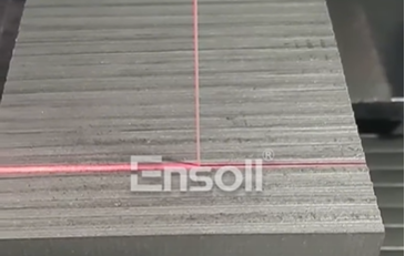
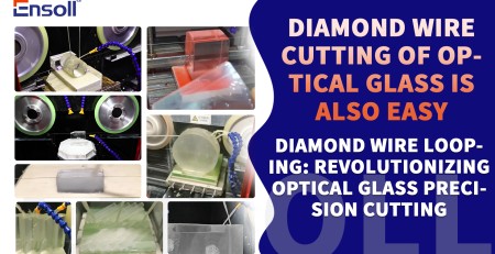
Видеовитрина:
Практический пример: Производство силовых модулей SiC

- Результат 1: Урожайность увеличена с 78% Кому 93%(Снижение количества отказов, вызванных трещинами).
- Результат 2: Достигнутая скорость резки 500мм/минс алмазной проволокой 0,3 мкм
Выбор правильной алмазной канатной пилы
Для применений на основе SiC/GaN, Приоритеты:
- Диаметр проволоки: 0.1–0,3 мм для чистовой отделки.
- Размер алмазной зернистости: 10–20 мкм для баланса между скоростью и качеством поверхности.
- Устойчивость машины: Вибрация <0.1μm для предотвращения микротрещин.
Будущие тренды
- Гибридная резка: Комбинация алмазной проволоки с лазерным предварительным нарезанием канавок для гетерогенная интеграция.
- Управление технологическими процессами на основе искусственного интеллекта: Корректировка в режиме реального времени для Резка без дефектов.
Заключение: Проложить путь в будущее
Пильный инструмент с алмазной проволокой является гораздо большим, чем просто инструмент для резки карбида кремния; это критически важная технология, открывающая возможности. Обеспечивая возможность резать этот сверхтвёрдый материал с непревзойденной точностью и аккуратностью, это напрямую способствует развитию технологий, которые делают наш мир более электрифицированным, связанным, и энергоэффективным. Поскольку спрос на подложки из SiC растет как по размеру, так и по количеству, развитие технологии алмазной проволоки — в направлении ещё более тонких проволок, умного контроля натяжения, и большей производительности — будет продолжать оставаться необходимым для обеспечения устойчивого, высокотехнологичного будущего.
Часто задаваемые вопросы
Какой лучший инструмент для резки карбида кремния?
Алмазная канатная пила. SiC находится близко к алмазу по твёрдости, поэтому только алмазный абразив эффективно его режет, а непрерывное действие проволоки с низкой силой предотвращает сколы и термическое повреждение, которые вызывают лезвия и лазеры.
Почему карбид кремния трудно резать?
Твердость по Моосу около 9,2–9,5 в сочетании с хрупкостью: Механическое воздействие вызывает сколы кромки, а тепло лазера — микротрещины. Какой бы метод вы ни выбрали, один из этих двух видов разрушения необходимо устранить при проектировании.
Повреждает ли лазерная резка SiC?
Да. Лазерная абляция оставляет зону, подверженную воздействию тепла, и переплавленный слой, который необходимо шлифовать, что увеличивает как стоимость, так и потери выхода продукции.
Сколько сколов кромки оставляет лезвие при резке SiC?
Обычная резка лезвием обычно вызывает дефекты кромки, превышающие 20 мкм. На силовых устройствах и высокочастотных чипах эти сколы напрямую уменьшают выход продукции, что является основной причиной перехода фабрик на алмазные проволоки.
Какое улучшение выхода продукции может дать алмазная проволока по сравнению с лазерной резкой SiC?
In a SiC power module line that switched from laser to diamond wire cutting for SiC MOSFETs, yield rose from 78% Кому 93% while running at 500 мм/мин. The improvement came from removing crack-induced failures rather than from cutting faster.
Can diamond wire saw cut gallium nitride (Гань) wafers?
Да, and the process window is different from SiC. GaN has lower hardness but high fracture toughness, so it tends to micro-crack rather than wear the tool. Use fine wire, moderate grit and very low machine vibration — below 0.1 µm — to keep the cut free of subsurface cracks.
Какую чистоту поверхности может обеспечить алмазная проволока на SiC?
С тонкой проволокой и стабильным натяжением, sub-micron Ra is achievable — often reducing or eliminating the lapping step entirely.
Насколько тонким может быть пропил при резке SiC?
Алмазная проволока может быть такой тонкой, что 0.2 миллиметр, дает чрезвычайно узкий путь реза. Учитывая стоимость слитков SiC, каждый сэкономленный миллиметр напрямую увеличивает количество пластин с каждого кристалла.
Какие диаметр проволоки и размер зерна подходят для резки SiC и GaN?
Для тонкой обработки SiC/GaN, 0.1– проволока 0,3 мм с алмазным зерном 10–20 мкм обеспечивает баланс между скоростью реза и качеством поверхности. Более тонкая проволока и зерно улучшают отделку и уменьшают потери на пропил, но замедляют резку.
Требуется ли охлаждающая жидкость при резке карбида кремния?
Да. Охлаждающая жидкость на водной основе удерживает рез в холоде и смывает отходы, что защищает как кристаллическую структуру на краю пластины, так и саму проволоку.
Как алмазная проволока сравнивается с резкой суспензией для SiC?
Пильные станки с суспензией медленные, тратят больше материала, and induce subsurface micro-cracks and high stress in the brittle crystal. Diamond wire sawing cuts faster, wastes less boule, and leaves a low-damage surface that shortens downstream grinding and polishing.
Технический контент проверен инженерной командой Ensoll — производителя алмазных проволочных петель с 10+ многолетним производственным опытом.