Precision cutting is paramount in semiconductor manufacturing because slicing damage propagates into every downstream process.
Different semiconductor materials need different cutting techniques: Silizium, Gaas, SiC and GaN each present distinct hardness and brittleness challenges.
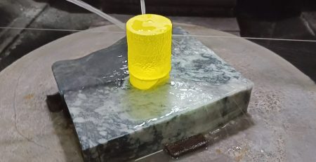
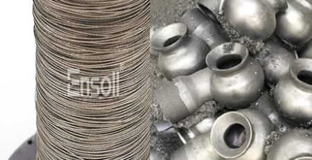
Diamond wire sawing has become the general-purpose answer across most semiconductor materials.
Auf dem Gebiet der Halbleiterfertigung, Präzision ist oberstes Gebot. Von Silizium zu Verbindungshalbleitern wie Galliumarsenid, the materials used in chip production require meticulous handling to ensure optimal performance. One critical aspect of this process is cutting these materials with utmost accuracy.
For silicon specifically, the shortlist narrows quickly — the comparison is set out inSiliziumwafer-Schneiden.
The Importance of Precision Cutting in Semiconductor Manufacturing
Precision cutting plays a pivotal role in semiconductor manufacturing by ensuring the integrity and performance of electronic devices. In this intricate process, even the slightest deviation can result in defects that compromise the functionality of semiconductors.
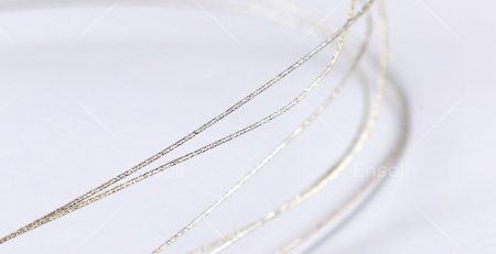
Precision cutting techniques such as laser cutting, diamond wire saw loop, and plasma etching enable manufacturers to achieve accurate dimensions and smooth surfaces critical for semiconductor components.
By maintaining tight tolerances and minimizing material wastage, precision cutting not only enhances the quality of semiconductor products but also contributes to efficiency and cost-effectiveness in the production process.
Letzten Endes, the importance of precision cutting in semiconductor manufacturing cannot be overstated, as it underpins the reliability and functionality of the electronic devices that power our modern world.
Common Semiconductor Materials and Their Cutting Techniques
Semiconductor materials are the bedrock of modern electronics, each demanding precise cutting techniques to unleash their full potential. Among these methods, dasDiamant-Drahtschneidemaschineemerges as a game-changer in semiconductor fabrication.
Silizium (Si):
Silizium, the workhorse of the semiconductor industry, is often cut using diamond wire cutting machines. This method ensures clean cuts with minimal damage, vital for producing integrated circuits and microchips.
For compounds like gallium arsenide, known for its use in high-frequency applications, the diamond wire cutting machine excels. Its precision and low heat generation make it ideal for shaping GaAs components with intricate patterns.
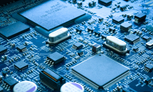
Gan, valued for its efficiency in power electronics and LEDs, benefits from the diamond wire cutting machine’s capabilities. This technique allows for precise cutting of GaN substrates, wesentlich für Hochleistungs-Halbleitergeräte.
Best Practices für das Schneiden von Halbleitermaterialien
Präzisionsgeräte:
Investieren Sie in hochwertige Schneidwerkzeuge und Maschinen, um genaue und saubere Schnitte zu gewährleisten.
Temperaturkontrolle:
Halten Sie optimale Temperaturbedingungen während des Schneidprozesses ein, um Materialschäden zu verhindern.
Nachbearbeitungsprüfung:
Führen Sie nach dem Schneiden gründliche Inspektionen durch, um die Qualität und Integrität der Materialien zu gewährleisten.
Schlussfolgerung
Im dynamischen Umfeld der Halbleiterfertigung, das Schneiden von Materialien stellt einen entscheidenden Schritt im Produktionsprozess dar. Durch die Anwendung der besten Schneidmethoden und -praktiken, können Hersteller die Qualität, Präzision, und Zuverlässigkeit von Halbleitergeräten sicherstellen, Innovationen und Fortschritte in der Branche vorantreiben.
Durch diesen Leitfaden, we aim to shed light on the significance of precision cutting in semiconductor manufacturing and provide insights into the best practices and techniques for achieving optimal results. Remember, in the world of semiconductors, every cut counts towards a brighter, more interconnected future.
Häufig gestellte Fragen
What is the best cutting method for semiconductor materials?
For most semiconductor crystals, diamond wire sawing offers the best combination of narrow kerf, low sub-surface damage and throughput; brittle compounds like GaAs especially benefit from its low cutting force.
Why do different semiconductors need different cutting techniques?
They differ in hardness, brittleness and thermal sensitivity — silicon is well understood, while SiC and GaN are far harder, and GaAs is softer but extremely fragile.
Warum ist präzises Schneiden in der Halbleiterfertigung so wichtig?
Oberflächenschäden und Dickenabweichungen, die beim Schneiden entstehen, setzen sich beim Planschleifen fort, Polieren und Lithografie, und beeinflussen direkt den Geräteausschuss.
Technische Inhalte geprüft vom Ensoll-Engineering-Team – einem Hersteller von Diamantdraht-Schleifen 10+ Jahre der Produktionserfahrung.
Achat, mit seinen faszinierenden Bändern und lebendigen Farben, ist ein Edelstein, der Handwerker und Sammler seit Jahrhunderten begeistert. Aber,... mehr lesen
Mit der kontinuierlichen Weiterentwicklung der Technologie, Die Vorteile der Diamantdrahtschlaufe in der spanenden Industrie werden immer größer.. mehr lesen
Siliziumcarbid (Sic), bekannt für seine außergewöhnliche Härte und Haltbarkeit, ist in verschiedenen Branchen weit verbreitet. Um dies effektiv zu reduzieren... mehr lesen
Wichtige Erkenntnisse
Kompakte einkernige Diamantdrahtschleifenmaschinen wie die ESV-3S bringen das Schneiden von Solarzellen in Reichweite von Laboren und... mehr lesen
Diamant-Drahtschlaufen werden mit fortschrittlichen Herstellungsverfahren hergestellt, bei denen Diamanten in eine Drahtschlaufe eingebettet werden. Das... mehr lesen
Wesentliche Erkenntnisse
Die Zero-Chipping-Kantentechnologie verwendet ultradünne Diamantdrahtschlaufen, um mechanische Belastungen zu minimieren, glatte, splitterfreie Kanten zu erzeugen, höhere... mehr lesen
Key Takeaways
Magnetic materials fall into three families: Dauermagnete (NdFeB, SmCo, AlNiCo, Ferrit), Weiche Magnetmaterialien (Siliziumstahl, Weicher Ferrit, Amorph.... mehr lesen
In der Welt des Präzisionsschneidens, Die Diamantdrahtsägetechnologie zeichnet sich als revolutionäre Methode aus, die die Art und Weise, wie.... mehr lesen
Im wettbewerbsorientierten Golf, Die Präzision der Ausrüstung wirkt sich direkt auf die Leistung aus. Während sich Golfer auf Schwungtechnik und Schlägerwahl konzentrieren, ein Durchbruch in der Fertigung... mehr lesen
In der Welt der Edelstein- und Hartstoffbearbeitung, Präzision ist nicht nur ein Luxus – sie ist eine absolute Notwendigkeit. Seit Jahrhunderten,... mehr lesen


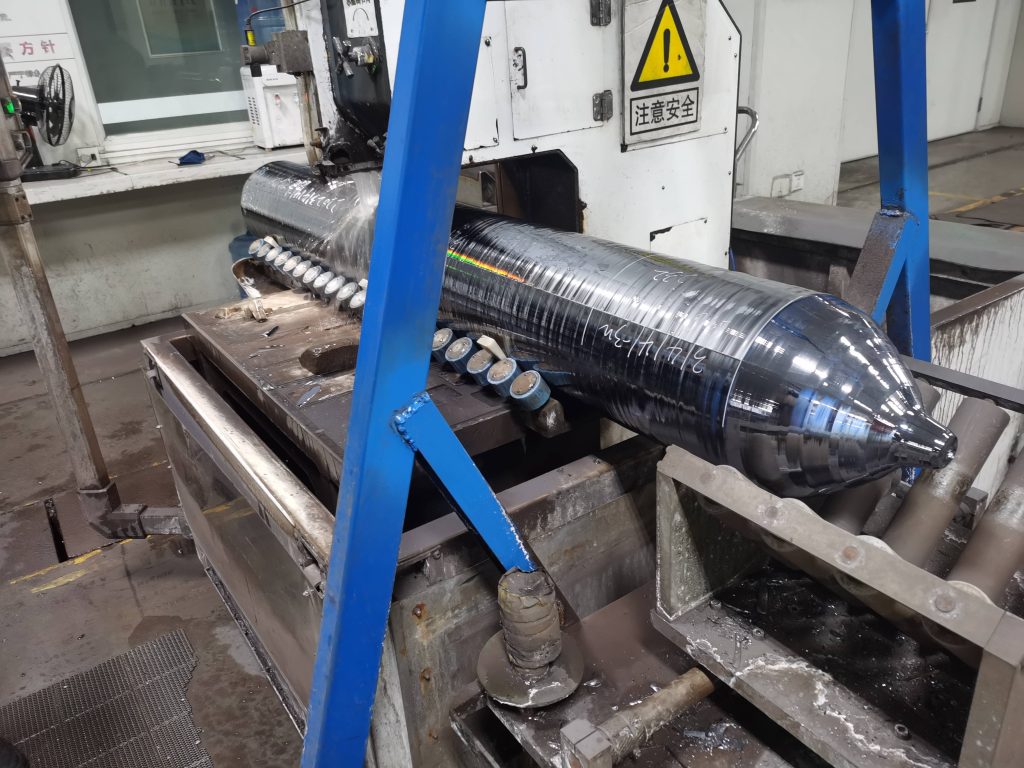


 Gan, valued for its efficiency in power electronics and LEDs, benefits from the diamond wire cutting machine’s capabilities. This technique allows for precise cutting of GaN substrates, wesentlich für Hochleistungs-Halbleitergeräte.