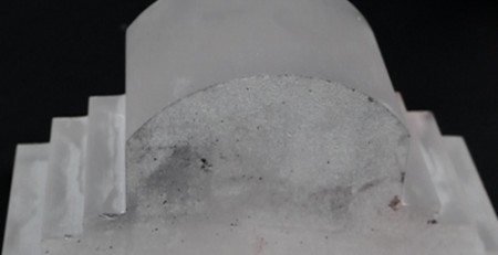
Silicon Ingot Processing in Semiconductor Industry
- Dans la préparation de plaquettes semi-conductrices, single-crystal silicon ingots are processed into bare wafers with high surface accuracy for lithography.
- Le flux de traitement de lingots comprend le découpage, broyage, Trancher, Chanfreinage, le lapage et le polissage, avec la fixation de la qualité de coupe influençant la charge de travail en aval.
À l’étape de préparation de la plaquette de silicium monocristallin, les lingots de silicium doivent être transformés en plaquettes de silicium brutes ou plaquettes nues avec une grande précision et qualité de surface afin de préparer la planarisation pour la lithographie et d'autres processus dans la première moitié du processus de CI. Une surface de substrat ultra-lisse et sans dommage est requise ici.
Pour les plaquettes de silicium d’un diamètre de ≤200 mm, Le processus traditionnel de traitement des plaquettes de silicium est:
Croissance monocristalline → découpage → meulage du diamètre extérieur du lingot → traitement des bords plats ou rainure en V → tranchage → chanfreinage → meulage → gravure → polissage → nettoyage → emballage .

Découpage : L'objectif est de couper la tête et la queue du lingot de silicium monocristallin et la partie qui dépasse la spécification du client, segment the single crystal silicon rod into the length that the slicing equipment can handle, and cut the test piece to measure the resistivity and oxygen content of the single crystal silicon rod. quantity.
This process traditionally uses a diamond band saw or a single diamond wire to truncate. Ces dernières années, a large-scale replacement of traditional truncation equipment has emerged after the emergence of endless diamond wire cutting .
Outer diameter grinding: Since the outer diameter surface of the single crystal silicon rod is not flat and the diameter is larger than the specified diameter specification of the final polished wafer, a more accurate diameter can be obtained by outer diameter rolling.
Flat edge or V-groove processing: Il est spécifié qu'il doit être traité jusqu'au plan de référence, et le bord plat ou la rainure en V avec une direction cristallographique spécifique sur le Silicium monocristallin support.
Tranchage: fait référence à la découpe d'un cristal simple en fines tranches avec des dimensions géométriques précises.
Chanfreinage: fait référence à l'élagage du bord tranchant de la plaquette découpée en une forme arquée pour éviter les fissures du bord de la plaquette et les défauts de qualité
Broyage: fait référence à l'élimination des marques de scie et des couches de dommages en surface causées par le découpage et le meulage à la roue par meulage, modifiant efficacement la déformation, la planéité et le parallélisme d'une plaquette de silicium produit unique, et atteignant les spécifications pouvant être traitées par un processus de polissage.
Contactez-nous pour plus d'informations
C'est l'étape immédiatement avant la découpe des tranches, et elle détermine quelle partie du lingot est utilisable.
Questions fréquemment posées
Quel est le flux de traitement des lingots de silicium dans l'industrie des semi-conducteurs?
Les lingots sont coupés à la longueur, meulés au diamètre précis, découpés en plaquettes, biseautés sur les bords, puis polissés par abrasion, gravés et polis jusqu'à obtenir la qualité de surface requise pour la lithographie.
Pourquoi la découpe est-elle une étape critique dans le traitement des lingots?
La découpe détermine la variation d'épaisseur de la plaquette et les dommages sous la surface, ce qui détermine la quantité d'abrasion et de polissage nécessaire pour obtenir une surface ultra-lisse, sans dommages.
Contenu technique examiné par l'équipe d'ingénierie d'Ensoll — un fabricant de boucles de fil diamanté avec 10+ des années d'expérience en production.