ニュース

従来の太陽電池製造プロセス

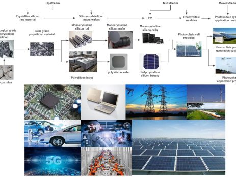
Traditional solar cell production process Key Takeaways Traditional solar cell production starts with silicon wafer manufacturing and proceeds through texturing, 拡散, エッチング, coating and metallization. Wafer slicing quality — kerf, TTV and surface damage — directly affects cell efficiency and yield. Before we always described the manufacturing principle and processing process of silicon wafers, today we will describe the production process of traditional solar cells. Traditional cell production can be mainly summarized into 6 ステップス. 従来のセル製造プロセスの観点から, it...
太陽光発電産業におけるシリコンウェーハのブーム

The boom of silicon wafers in the photovoltaic industry Key Takeaways Carbon-neutrality goals worldwide have made photovoltaics the fastest-growing source of demand for silicon wafers. PV wafer economics are driven by kerf loss and throughput, which is the main reason diamond wire replaced slurry saws across the industry. Larger wafer formats and thinner wafers are the PV industry's structural cost-reduction path, and both raise the bar for cutting precision. Under the background of the carbon neutralization goal and the accelerated application of global clean energy,...

2022 半導体ウェーハ業界の概要

2022 Semiconductor Wafer Industry Overview Key Takeaways Semiconductor silicon wafers are the carrier substrate for chip manufacturing, and the wafer industry is highly concentrated and technology-intensive. Industry development is driven by larger wafer diameters, tighter flatness specs and growing demand from logic, memory and power devices. 半導体シリコンウェーハは、チップを製造するためのキャリアです, 原料がシリコンであることからシリコンウェーハとも呼ばれます. 計画と管理不要のシリコン精製後, 浄化, 単結晶シリコン製造, ウェーハ成形およびその他のプロセス, it can enter the...

Diamond Wire Silicon Wafer Cutting Equipment Trends

1) High line speed and high production capacity support the reduction of single GW investment According to the theory of fracture mechanics and the properties of silicon materials, ダイヤモンド砥粒の最大切込みがシリコン材料の臨界切込みより大きい場合, 塑性切断から脆性破壊切断への移行が起こります. そこで, ダイヤモンド線荷重の許容範囲内, appropriately increasing the steel wire speed in the multi-wire cutting process is beneficial...

太陽光発電シリコンウェーハの寸法変化

Key Takeaways Photovoltaic silicon wafer sizes evolved from semiconductor wafer formats, with PV historically lagging semiconductors in dimension standards. Wafer dimensions keep growing (from 156 mm to 182/210 mm classes) because larger wafers cut module cost per watt. Larger and thinner wafers raise the precision bar for slicing equipment and diamond wire. 光起電力シリコンウェーハのサイズは、半導体シリコンウェーハに由来する. 開発の面で , 太陽光発電は半導体に遅れをとっている 1 宛先 2 世代. 何年にもわたって, the size of...

Silicon Ingot Processing in Semiconductor Industry

Key Takeaways In semiconductor wafer preparation, single-crystal silicon ingots are processed into bare wafers with high surface accuracy for lithography. The ingot processing flow includes cropping, 研削, スライス, 面取り, lapping and polishing, with slicing quality setting downstream workload. 単結晶シリコンウェーハ準備段階, シリコンインゴットは、ICプロセスの前半でリソグラフィーなどの平坦化に備えるために、高い表面精度と表面品質で生のシリコンウェーハまたはベアワファーに加工する必要があります. Ultra-smooth...