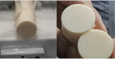
ダイヤモンドワイヤーループによるシリコンロッドの精密スライス
要約: This article presents a comprehensive study on the precision slicing of silicon rods using a ダイヤモンドワイヤーループ. The test workpiece was a φ330 mm × 500 mm silicon rod sourced from a European customer, sliced into 10 mm-thick wafers on an Ensoll ESC600-4T single-cantilever machine. We report the cutting parameters, cooling strategy, and quantitative quality metrics including Total Thickness Variation (TTV), dimensional tolerance, 表面粗さ (Ra), and edge chipping. The results demonstrate that an optimized diamond wire loop process can achieve stable, high-precision silicon slicing suitable for downstream semiconductor and photovoltaic applications.
- A φ330 mm × 500 mm silicon rod was sliced into 10 mm wafers on the Ensoll ESC600-4T diamond wire loop machine (0.50 mm wire, 38 メートル/秒, 210 N tension).
- Optimizing feed parameters cut TTV from 0.170 mm to 0.070 mm across three test runs.
- Average surface roughness stayed below 1 μm Ra with minimal edge chipping.
1. 紹介
Silicon is the backbone of the modern semiconductor and photovoltaic industries. Monocrystalline silicon wafers demand exceptionally tight tolerances: minimal thickness variation, low surface roughness, and near-zero edge chipping. Achieving these specifications on large-diameter silicon rods is challenging because silicon is both hard and brittle, with relatively low fracture toughness. During abrasive cutting, concentrated thermal and mechanical loads can trigger brittle fracture, propagate subsurface micro-cracks, and produce edge chipping and thickness inconsistency.
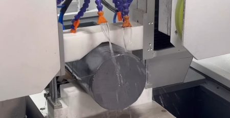
To address these challenges, Ensoll Tools designed a dedicated process for high-precision linear slicing of silicon rods. The approach combines continuous water cooling to suppress cutting-zone temperature rise, optimized feed parameters matched to the material, and a custom single-cantilever diamond wire loop cutting machine (ESC600-4T). By aligning machine structure, cooling conditions, and cutting parameters, the process minimizes thermal and mechanical damage to both the wafer surface and edges, delivering the dimensional accuracy, thickness uniformity, and surface quality required for advanced silicon applications.
2. Test Object and Material Properties
The workpiece for this study was supplied by a European customer (referred to as Customer F). The key material and geometry data are summarized below:
- Material: Silicon rod
- Hardness: Mohs ~6.0–6.5
- Workpiece dimensions: φ330 mm × 500 ミリメートル (L)
- Target slice thickness: 10 ミリメートル
Silicon’s combination of high hardness and brittleness makes it a classic representative of hard-and-brittle materials. Any cutting technology applied to silicon must simultaneously control abrasive wear, heat accumulation, and brittle-mode material removal.
The same hard-and-brittle behaviour sets the practical feed limit when cutting alumina ceramics, where chipping rather than tool wear is the binding constraint.
3. Machine and Wire Selection
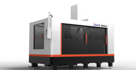
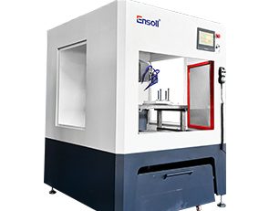
The cutting trials were performed on an Ensoll ESC600-4T single-cantilever diamond wire loop cutting machine. This model was developed specifically for large-diameter silicon-rod slicing, taking into account the material’s hardness, 脆性, and the geometric tolerances demanded by semiconductor-grade processing.
- Coolant: Water. Water offers high specific heat capacity and excellent convective heat transfer, making it ideal for reducing cutting-zone temperature and flushing away silicon debris. Continuous water supply improves interface cleanliness, cutting stability, and final surface quality.
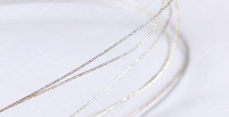
- Wire type: Fully electroplated diamond wire loop. The electroplated bond ensures high-density, uniform diamond-grain distribution and strong grain retention. This configuration maximizes effective cutting edges, improves wire durability, and reduces surface damage and edge chipping.

4. Cutting Method and Machine Advantages
The ESC600-4T integrates several structural and control features that directly benefit silicon-rod slicing:
- Gantry cutting architecture: A high-rigidity gantry frame drives the cutting assembly vertically. This layout maintains structural stability and motion accuracy throughout the cut, suppressing vibration and trajectory deviation. The result is improved perpendicularity and dimensional consistency across each slice.
- Moving-head, fixed-workpiece design: The cutting assembly moves while the silicon rod remains stationary. Eliminating workpiece motion preserves the machining reference and allows a more compact machine footprint for the same billet size.
- Adjustable V-support platform: An adaptable V-type support structure can be repositioned to match the rod diameter, ensuring stable clamping and accommodating a range of silicon-rod specifications.
- Hydraulic loading table: A hydraulic lift handles rod loading and positioning, reducing impact and positional drift during manual handling. The lift also retracts clear of the support structure during cutting, preventing interference.
- Intelligent tension control: The tension system continuously adjusts wire tension in response to run-time state and wire-diameter wear, keeping the diamond wire loop in a stable tension window. When idle, the system relaxes tension to minimize long-term load on both the wire and guide-wheel grooves; upon restart, working tension is restored rapidly.
5. Cutting Parameters and Cooling
The principal cutting parameters were selected based on the silicon material properties, ザ 10 mm target slice thickness, and preliminary process verification. The parameter set is summarized in Table 1.
| Parameter | Value |
|---|---|
| 線径 (ミリメートル) | 0.50 × 3,570 |
| 送り速度 (ミリメートル/分) | 15 / 18 / 25 |
| Cutting width (ミリメートル) | 330 |
| Wire tension (N) | 210 |
| Wire speed (メートル/秒) | 38 |
| Wire bow time (s) | 200 |
Water was supplied continuously as the coolant throughout all cuts. Three feed speeds were evaluated—15, 18, そして 25 mm/min—to investigate the influence of removal rate on slice quality.

6. 切削結果
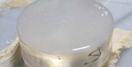
Three slices (labeled S01, S02, and S03) were produced and subjected to metrological inspection. Each sample was measured for Total Thickness Variation (TTV), dimensional tolerance, 表面粗さ (Ra), and edge chipping.

6.1 総厚変化 (TTV)
TTV was measured using a vacuum-chuck nine-point grid dual-probe thickness gauge. The equipment was thermally equilibrated and calibrated with certified thickness blocks before testing. Samples were cleaned in a dust-free environment, centered on the vacuum chuck, and held flat by negative pressure to minimize warpage-induced error.
| サンプル | Nine-point thickness (ミリメートル) | Tmax (ミリメートル) | Tmin (ミリメートル) | TTV (ミリメートル) |
|---|---|---|---|---|
| S01 | 9.780, 9.750, 9.760, 9.820, 9.650, 9.720, 9.790, 9.730, 9.770 | 9.820 | 9.650 | 0.170 |
| S02 | 9.926, 9.977, 9.952, 9.961, 9.936, 9.885, 9.948, 9.920, 9.950 | 9.977 | 9.885 | 0.092 |
| S03 | 10.006, 10.071, 10.075, 10.073, 10.005, 10.066, 10.032, 10.048, 10.058 | 10.075 | 10.005 | 0.070 |
評価: The nine-point TTV data show that S03 delivered the best thickness uniformity (0.070 ミリメートル), while S01 exhibited the largest variation (0.170 ミリメートル). As feed speed increased from 15 mm/min to 25 ミリメートル/分, TTV improved monotonically, suggesting that a moderately higher feed rate can stabilize the cutting process and reduce thickness fluctuation when combined with appropriate cooling and tension control.
6.2 Thickness Dimensional Tolerance
Thickness tolerance was evaluated against a nominal thickness of 10.000 mm using the same nine-point grid data. Positive and negative deviations were computed for each measurement point and summarized across all three slices.
| サンプル | Average thickness (ミリメートル) | Thickness deviation (ミリメートル) |
|---|---|---|
| S01 | 9.641 | −0.359 |
| S02 | 9.939 | −0.061 |
| S03 | 10.048 | +0.048 |
| Max positive deviation | +0.048 | — |
| Max negative deviation | −0.359 | — |
| Overall thickness tolerance | ±0.359 | — |
評価: The thickness deviations were predominantly negative. S01 showed a pronounced thin bias (−0.359 mm), which widened the overall tolerance band. S02 and S03 progressively approached the nominal dimension, indicating improved dimensional control stability at higher feed speeds. The trend confirms that feed-rate optimization is a critical lever for thickness accuracy in silicon wafer cutting.
6.3 Surface Roughness (Ra)
Surface roughness was measured with a stylus profilometer according to ISO 4287. The measurement direction was aligned with the dominant surface texture orientation. Three locations were inspected on each slice: center, left-mid, and right-mid.
| サンプル | Ra-1 (マイクロメートル) | Ra-2 (マイクロメートル) | Ra-3 (マイクロメートル) | Average Ra (マイクロメートル) |
|---|---|---|---|---|
| S01 | 0.860 | 0.640 | 0.690 | 0.730 |
| S02 | 0.910 | 0.960 | 0.680 | 0.850 |
| S03 | 0.760 | 0.670 | 0.800 | 0.743 |
評価: Average Ra values ranged from 0.730 μm to 0.850 マイクロメートル, with an overall spread of 0.640–0.960 μm. The small variation between measurement positions on each slice indicates a uniform surface texture, confirming that the diamond wire loop run and material removal remained stable throughout the cut. These Ra levels are consistent with high-quality abrasive slicing of silicon and compare favorably with results reported in our precision slicing of metal tubes case study.
6.4 エッジチッピング
Edge chipping was quantified by optical microscopy on all four edges of each slice. Samples were cleaned, the microscope scale was calibrated, and all four sides were scanned sequentially.
| サンプル | Position 1 (マイクロメートル) | Position 2 (マイクロメートル) | Position 3 (マイクロメートル) | Position 4 (マイクロメートル) | Max chipping (マイクロメートル) |
|---|---|---|---|---|---|
| S01 | 5.6 | 7.2 | 6.4 | 8.1 | 8.1 |
| S02 | 6.3 | 8.5 | 7.1 | 9.2 | 9.2 |
| S03 | 5.1 | 6.8 | 7.4 | 8.6 | 8.6 |
評価: Chipping sizes ranged from 5.1 μm to 9.2 マイクロメートル, with mean maximum chipping of 8.6 マイクロメートル. The relatively narrow distribution across all samples indicates stable material removal at the kerf boundary. Edge integrity at this level is acceptable for many semiconductor preprocessing steps and can be further improved with parameter refinement.

7. 結論
The silicon-rod slicing trials demonstrate that a well-matched combination of machine architecture, coolant system, and cutting parameters can deliver high-precision results on large-diameter silicon billets. The key findings are:
Shops specifying equipment for large-diameter work can compare gantry and cantilever architectures in our overview of the ダイアモンドワイヤーソー切断機.
- Machine structure matters. The single-cantilever ESC600-4T gantry design provides the motion stability and clamping adaptability needed for φ330 mm silicon rods. By isolating machine vibration from the wire trajectory, the cantilever layout establishes a solid foundation for thickness control and cutting consistency.
- Cooling is non-negotiable. Continuous water cooling effectively suppresses cutting-zone temperature rise, flushes abrasive debris, and maintains a clean wire–workpiece interface. The reduction in thermal load and particulate contamination directly translates to more stable cutting and better surface integrity.
- Feed-rate optimization pays off. Raising the feed speed from 15 mm/min to 25 mm/min progressively reduced TTV from 0.170 mm to 0.070 ミリメートル. This confirms that, within the tested window, a faster feed can stabilize the material-removal process and improve thickness uniformity when paired with adequate cooling and tension control.
Collectively, the TTV, thickness tolerance, 表面粗さ (Ra), and chipping data validate that the optimized ダイヤモンドワイヤーループ process on the ESC600-4T is capable of producing silicon slices that meet the stringent requirements of photovoltaic and semiconductor downstream processing. The results provide a practical process baseline for engineering-scale silicon-rod slicing and can be adapted to other hard-and-brittle materials of comparable hardness and geometry.
For more information on Ensoll’s diamond wire loop solutions for silicon, 磁性材料, 陶芸, と金属, explore our precision slicing guides or contact our engineering team.
These results sit alongside our wider work on silicon wafer slicing, where the same parameters are tuned for thinner wafers.よくある質問
What TTV can a diamond wire loop achieve when slicing silicon rods?
In this ESC600-4T test on a φ330 mm silicon rod, total thickness variation (TTV) improved from 0.170 mm to 0.070 mm as feed parameters were optimized across three runs.
What surface roughness does diamond wire loop slicing produce on silicon?
Average Ra stayed below 1 μm across samples in this study — smooth enough to reduce or eliminate downstream lapping for many applications.
Which machine was used for this silicon rod slicing study?
The Ensoll ESC600-4T single-cantilever diamond wire loop cutting machine, running a 0.50 mm diamond wire loop at 38 m/s wire speed and 210 N tension.
Why use a diamond wire loop instead of a slurry saw for silicon rods?
The loop cuts with fixed diamond abrasive in a water-cooled, single-direction pass, giving a narrower kerf, less sub-surface damage, and shorter cycle times than loose-abrasive slurry sawing.
Technical content reviewed by the Ensoll engineering team — a diamond wire loop manufacturer with 10+ years of production experience.