Silicon Ingot Processing in Semiconductor Industry
- In semiconductor wafer preparation, single-crystal silicon ingots are processed into bare wafers with high surface accuracy for lithography.
- The ingot processing flow includes cropping, grinding, slicing, chamfering, lapping and polishing, with slicing quality setting downstream workload.
In the single-crystal silicon wafer preparation stage, the silicon ingots need to be processed into raw silicon wafers or barewa-fers with high surface accuracy and surface quality to prepare for planarization for lithography and other processes in the first half of the IC process. Ultra-smooth and damage-free substrate surface are required here.
For silicon wafers with a diameter of ≤200mm, the traditional silicon wafer processing process is:
single crystal growth → cropping → outer diameter barrel grinding → flat edge or V-groove treatment → wafering → chamfering → grinding → etching → polishing → cleaning → packaging .

Cropping : The purpose is to cut off the head and tail of the single crystal silicon ingot and the part that exceeds the customer’s specification, segment the single crystal silicon rod into the length that the slicing equipment can handle, and cut the test piece to measure the resistivity and oxygen content of the single crystal silicon rod. quantity.
This process traditionally uses a diamond band saw or a single diamond wire to truncate. In recent years, a large-scale replacement of traditional truncation equipment has emerged after the emergence of endless diamond wire cutting .
Outer diameter grinding: Since the outer diameter surface of the single crystal silicon rod is not flat and the diameter is larger than the specified diameter specification of the final polished wafer, a more accurate diameter can be obtained by outer diameter rolling.
Flat edge or V-groove processing: It is specified to be processed to the reference plane, and the flat edge or V-groove with a specific crystallographic direction on the monocrystalline silicon holder.
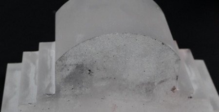
Wafering: refers to cutting a single crystal silicon rod into thin slices with precise geometric dimensions.
Chamfering: refers to trimming the sharp edge of the cut wafer into an arc shape to prevent chip edge cracking and quality defects
Grinding: refers to the removal of saw marks and surface damage layers caused by slicing and wheel grinding by grinding, effectively changing the warpage, flatness and parallelism of a single-product silicon wafer, and reaching the specifications that can be handled by a polishing process.
Contact us for more info
This is the stage immediately before wafer slicing, and it decides how much of the ingot is usable.
Frequently Asked Questions
What is the processing flow of silicon ingots in the semiconductor industry?
Ingots are cropped to length, ground to precise diameter, sliced into wafers, edge-chamfered, then lapped, etched and polished to the surface quality that lithography requires.
Why is slicing a critical step in ingot processing?
Slicing determines the wafer’s thickness variation and sub-surface damage, which sets how much lapping and polishing is needed to reach an ultra-smooth, damage-free surface.
Technical content reviewed by the Ensoll engineering team — a diamond wire loop manufacturer with 10+ years of production experience.