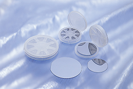
A semiconductor chip, comumente referido como um circuito integrado, is a semiconductor device fabricated on a semiconductor wafer through processes such as etching, wiring, and patterning to achieve specific functions. Beyond silicon chips, common semiconductor materials include gallium arsenide, nitreto de galio, and silicon carbide.
Última análise: Setembro 2026
Principais Conclusões
Semiconductors are materials with conductivity between conductors and insulators, forming the basis of all integrated circuits.
Beyond silicon, key semiconductor types include gallium arsenide (GaAs), nitreto de galio (Represa) and silicon carbide (Sic), each with distinct application niches.
GaAs serves RF and optoelectronics, GaN serves high-frequency power, and SiC serves high-voltage, high-temperature power devices.
The semiconductor manufacturing process is akin to turning base materials into gold, primarily involving a series of treatments on silicon wafers. In essence, through epitaxial growth, photolithography, etching, doping, and polishing, the required circuits are formed on the silicon wafer, transforming it into a chip.
Types of Semiconductors
Semiconductor materials are electronic materials used in the production of semiconductor devices and integrated circuits, forming the foundation of the semiconductor industry.
With the emergence of new semiconductor materials, advancements in power electronics technology, and improvements in manufacturing processes, semiconductors have undergone three generations of changes. Arsénio de gálio (GaAs) and gallium nitride (Represa), as well as silicon carbide (Sic) semicondutores, represent the second and third generations of semiconductors, respectively.
Compared to the first-generation semiconductor silicon (Si), these materials exhibit superior performance in aspects such as high frequency and high temperature.
Compound semiconductor chips, known for their excellent high-frequency performance, are commonly used in the production of power semiconductors, with their applications becoming increasingly widespread. Through techniques such as frequency conversion, voltage transformation, current modulation, power amplification, and management, these chips serve two primary functions: amplification and switching.
Atualmente, over 75% of electrical energy applications require power conversion before being supplied to devices. Their applications continue to expand.
Amplification involves converting low-frequency power into high-frequency power, leveraging amplification to drive motors with low power efficiently. Switching entails toggling circuits on and off, with faster switching speeds enabling precise control.
Amplification: Converting low-frequency power into high-frequency power, making full use of amplification allows for driving motors with low power effectively.
Switching: Alternar o circuito ligado e desligado, quanto maior a velocidade de comutação, mais controlo preciso pode ser alcançado.
Semicondutor de Arsénio de Gálio
Os chips semicondutores de arsénio de gálio são principalmente usados em dispositivos de potência de micro-ondas, que operam na gama de frequências de micro-ondas (entre 300 e 300,000 megahertz). Devido às limitações físicas inerentes ao silício (Si), só pode ser aplicado em frequências abaixo de 1 GHz. Contudo, nos últimos anos, o rápido desenvolvimento de produtos de comunicação sem fios de alta frequência impulsionou o arsénio de gálio para a vanguarda, mostrando características como altas frequências de operação, taxas de mobilidade eletrónica, resistência à radiação natural, e baixo consumo energético, fazendo com que seja amplamente utilizado no campo da comunicação por micro-ondas.
Dadas as características de transmissão de alta frequência do arsénio de gálio, it has seen rapid growth not only in mobile phone applications but also in WiFi modules embedded in laptops, tablets, fixed network wireless transmission, as well as fiber optic communication, satellite communication, point-to-point microwave communication, cable television, automotive navigation systems, and collision avoidance systems. These applications often employ varying numbers of power amplifiers (ranging from 1 Para 4 chips), driving the significant advancement of gallium arsenide.
Gallium Nitride Semiconductor
Gallium nitride material, with a bandgap width of 3.4 eV, is considered a third-generation semiconductor material along with materials like SiC and diamond, known as wide-bandgap semiconductors. Due to its advantages such as a wide bandgap, high breakdown field, large saturation electron velocity, alta condutividade térmica, baixa constante dielétrica, Estabilidade química, and strong radiation resistance, o nitreto de gálio tornou-se um dos materiais preferidos para dispositivos de micro-ondas de alta temperatura, alta frequência, e alta potência.
Comparação do Nitreto de Gálio (Represa) com Arsénio de Gálio (GaAs) e Silício (Si):
A crescente procura por dispositivos semicondutores de alta velocidade, alta temperatura, e alta potência levou à adoção gradual do material nitreto de gálio no mercado de semicondutores. As suas principais áreas de aplicação incluem:
Setor de Energia Renovável:
No campo da energia renovável, o nitreto de gálio desempenha um papel extremamente importante na integração da energia eólica e solar na rede elétrica e na redução das perdas de transmissão. Energia verde, veículos elétricos, iluminação eletrónica verde, e outras áreas emergentes estão a tornar-se novos pontos quentes para aplicações no mercado de dispositivos de potência, com forte procura.
Setor de Equipamentos de Comunicação e Informação:
Os transístores de nitreto de gálio melhorados apresentam alta resistência à radiação, tornando-os adequados para sistemas de energia e comunicação em satélites de comunicação e científicos. Comunicação ponto a ponto, satellite communication, vários radares, e novas aplicações industriais/defesa irão beneficiar da aplicação destes dispositivos de nitreto de gálio de alta potência.
4Indústrias C:
Espera-se que os principais produtos nacionais de TI mantenham uma forte procura no mercado, com produtos tradicionais como computadores portáteis, monitores, impressoras, televisores, sistemas de home theater, e leitores Blu-ray, bem como eletrónica automóvel emergente, prevê-se um crescimento sustentado no futuro. À medida que a capacidade de produção de produtos eletrónicos, como ar-condicionado e motores energeticamente eficientes, se desloca para a China continental, espera-se que a procura por semicondutores de potência duplique.
Setor de Redes Inteligentes:
Power semiconductors play a crucial role in improving the overall energy efficiency of the entire power supply chain—from generation, transmission, and distribution to end-user consumption—in the field of smart grids.
Silicon Carbide Semiconductor
Carboneto de silício (Sic) has become one of the most prominent semiconductor materials due to its outstanding performance under high temperature, high pressure, and high frequency conditions. It is widely used in power conversion devices such as AC-DC converters and is expected to gradually replace silicon comprehensively in the field of semiconductor power devices, heralding the dawn of the Silicon Carbide Semiconductor era.
Compared to silicon devices, SiC semiconductor chips can reduce power losses by nearly 50%, effectively enhancing power conversion efficiency. SiC devices, com a sua elevada eficiência de conversão e baixa geração de calor, podem reduzir o tamanho dos sistemas de arrefecimento, levando a uma redução global dos dispositivos de conversão de energia. Isto é de grande importância para sistemas como veículos de novas energias que requerem numerosos dispositivos de conversão de energia. Portanto, para sistemas que exigem alta eficiência de conversão e densidade de potência, os dispositivos de SiC oferecem vantagens incomparáveis e são a escolha preferida.
Devido ao seu desempenho excecional, o carboneto de silício é particularmente adequado para aplicações que exigem conversão de energia de alta potência, tais como perfuração de poços profundos, inversores solares (para conversão de DC para AC), inversores de energia eólica, veículos elétricos e híbridos, acionamentos industriais, e sistemas de tracção de metro ligeiro.
Método de Fabricação:
O processo de fabricação de semicondutores é semelhante a transformar chumbo em ouro, primarily involving a series of treatments on silicon wafers. While a detailed explanation can be quite complex, in simple terms, it involves epitaxial growth, photolithography, etching, doping, and polishing to create the required circuits on the silicon wafer, transforming it into a chip. Steps like photolithography and etching still rely on foreign technologies and the use of foreign patents
Semiconductor processing methods
Four Cutting Technologies: A Comparative Overview:
1. Corte em Loop com Fio de Diamante
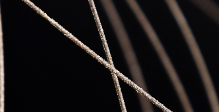
Principle: A fast-moving loop of wire, revestido com partículas de diamante, acts as a cutting tool, grinding through the material. Coolant is often used.
Key Advantage:Low stress, alta precisão, minimal material waste. O “flexible” wire is gentle on brittle materials, enabling clean cuts with almost no edge chipping. It is the preferred method for slicing high-value, duros, brittle materials like SiC, Represa, safira, e vidro ópticointo thin wafers.
Limitation:Limited cutting speed. As a grinding process, its material removal rate is slower than thermal methods like laser cutting, making it less efficient for high-volume or rough cutting jobs.
2. Diamond Saw Blade Cutting
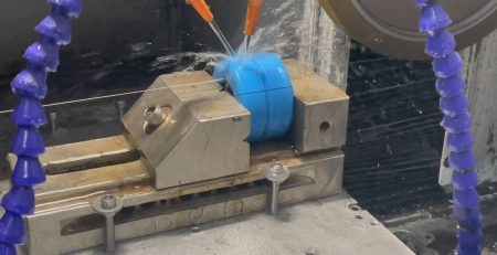
Principle:A rotating circular blade with a diamond-coated edge cuts through the material, similar to a precision stone cutter.
Key Advantage:Proven technology, Alta eficiência, relatively low cost. It’s the standard method for rough cutting and sizing blocks of silicon and ceramic.
Limitation:High mechanical impact. It can easily cause edge chipping and internal stress or micro-cracks, making it unsuitable for finishing ultra-thin, ultra-hard, or high-value materials.
3. Corte a Laser
Principle:A focused, high-energy laser beam melts, vaporizes, or alters the material, with a gas jet removing the debris.
Key Advantage:Non-contact, no tool wear, very fast, highly flexible. It easily handles complex 2D shapes and can perform “stealth dicing” (separação através de modificação interna), tornando-o ideal para o corte de pastilhas e moldagem de silício, safira, e vidro.
Limitation: Cria uma zona afetada pelo calor que pode alterar as propriedades do material na borda cortada. Pode ter dificuldades com materiais altamente refletivos (por exemplo,, cobre puro) ou materiais transparentes. O equipamento é caro.
4. Corte por Descarga Elétrica (Eletroerosão a fio)
Principle: Descargas de faísca controladas entre um eletrodo de fio fino e a peça geram calor intenso, derretendo e vaporizando localmente o material.
Key Advantage: Corta qualquer material condutor independentemente da dureza (por exemplo,, aço endurecido, carboneto de tungstênio, cerâmicas condutoras). Alcança precisão muito elevada e pode criar formas complexas.
Limitation: Só funciona em materiais condutores. O processo é lento, e deixa uma camada recompactada na superfície cortada.
Resumo & Guia de Seleção
Não existe uma única “melhor” tecnologia — cada uma é mais adequada para tarefas específicas:
For ultimate cut quality and minimal loss when slicing hard, brittle wafers (por exemplo,, Sic): ChooseLaço de fio diamantado Corte.
For efficient, low-cost rough cutting of hard, brittle blocks: Choose Diamond Saw Blade Cutting.
For high-speed cutting of complex 2D shapes in various materials (including non-metals): Choose Laser Cutting.
For machining intricate shapes in very hard, conductive materials (por exemplo,, molds): Electrical Discharge Cutting is the only choice.
Current Situation:
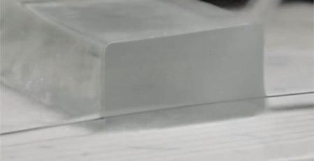
Atualmente, many technologies require a fresher perspective to be infused, as each step in the process could potentially lead to significant advancements. Regarding one specific aspect, we conducted a experiment on cutting 12-inch ingots two weeks ago. We utilizedEnsolltoolsLimited’sserra de fio de diamante tecnologia, where the wire marks are nearly invisible, and the flatness can be controlled within 3 micrómetros. Este método resolve muitos problemas relacionados com o corte de superfícies côncavas de semicondutores, reduzindo significativamente a dificuldade do polimento subsequente e o consumo de material.
Independentemente do tipo de semicondutor envolvido, os dispositivos ainda começam a sua vida no processo de corte da pastilha.
Perguntas Frequentes
O que é um semicondutor?
Um semicondutor é um material cuja condutividade elétrica se situa entre a de um condutor e a de um isolador e pode ser controlada por dopagem, tornando-o a base dos circuitos integrados.
Quais são os principais tipos de materiais semicondutores?
O silício domina os CI gerais; os semicondutores compostos incluem arseneto de gálio (RF, optoeletrónica), nitreto de galio (alta frequência de potência) and silicon carbide (alta tensão, alta potência em alta temperatura).
Onde são usados semicondutores de SiC e GaN?
O SiC é usado em inversores de veículos elétricos e em módulos de potência de alta tensão, enquanto o GaN é usado em carregadores rápidos, Amplificadores de potência RF e infraestrutura 5G.
Principais Conclusões
O corte a laser é sem contacto e rápido, mas a sua zona afetada pelo calor pode criar microfissuras que reduzem a eficiência da célula solar.
Fio de diamante.... leia mais
O corte de arame em loop diamantado possui várias vantagens significativas no campo do processamento de materiais magnéticos, tornando-o um corte ideal... leia mais
Principais Conclusões
O vidro ótico é fabricado a partir de uma composição precisa de silicatos e óxidos metálicos para alta transparência e luz mínima... leia mais
Ímãs de neodímio, também conhecidos como ímãs NdFeB, possuem uma força incrível e são amplamente utilizados em uma variedade de aplicações. Contudo,... leia mais
Principais Conclusões
Ferrite (cerâmica) são óxido de ferro sinterizado com carbonato de estrôncio ou bário: baratos, resistentes à corrosão e estáveis até 250... leia mais
Principais Conclusões
Métodos tradicionais de corte de pneus - tesouras hidráulicas, serras de fita, lasers e ferramentas manuais - todos têm dificuldade com cortes irregulares,... leia mais
Como fabricante líder global de ferramentas e equipamentos industriais, Nossa empresa tem muito orgulho em nossas instalações de produção de última geração... leia mais