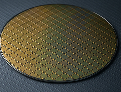
Semiconductor wafer slicing is a critical IC manufacturing step where precision and surface integrity determine device yield.
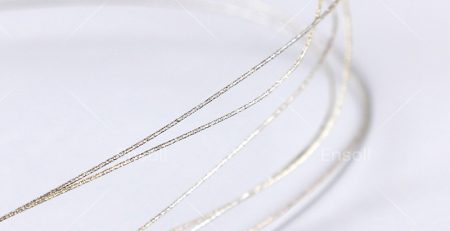
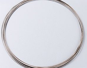
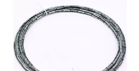
A diamond cutting wire loop is a closed loop of diamond-coated wire that slices ingots with ultra-precise, mínima perda de kerf.
As suas principais vantagens são menor stress térmico e mecânico do que o corte a laser ou com lâmina, o que é mais importante à medida que as pastilhas se tornam mais finas.
Semicondutor fatiagem de pastilhas é um processo crítico na fabricação de circuitos integrados (Ics) e outros dispositivos microeletrônicos. Precisão e eficiência são primordiais, pois mesmo pequenos defeitos podem levar a problemas significativos de desempenho no produto final. Entre as várias tecnologias de corte disponíveis, O laço de fio de corte diamantado surgiu como um método superior devido à sua precisão excepcional, perda mínima de material, e vida útil prolongada da ferramenta.
Neste artigo, we will explore whycorte de arame diamantadois becoming the preferred choice for semiconductor wafer dicing and how it outperforms traditional methods like blade sawing and laser cutting.
The Challenges of Semiconductor Wafer Cutting
Pastilhas de semicondutor, typically made of silicon, are extremely thin and fragile. The cutting process must ensure high precision with minimal kerf width and chipping, low thermal damage to prevent microcracks, and high throughput for cost-effective production.
Traditional methods such as mechanical blade sawing can cause microcracks and material loss, while laser cutting may introduce thermal stress. This is where diamond cutting wire loop technology excels.
What Is Diamond Cutting Wire Loop?
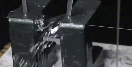
A diamond cutting wire loop is a thin, flexible wire embedded with diamond abrasive particles. It operates by continuously moving the wire across the wafer, enabling precise and smooth cuts with minimal mechanical stress. .
Key Advantages of Diamond Wire Cutting
Ultra-Precise Cutting with Minimal Kerf Loss
Diamond wire cutting produces an extremely narrow kerf, as small as 20-30 µm, allowing for higher wafer yield compared to blade sawing. The fine abrasive action reduces chipping and edge defects, crucial for delicate wafers.
Reduced Material Waste
Since the wire is much thinner than a saw blade, less silicon is wasted, improving material utilization and lowering production costs.
Lower Thermal and Mechanical Stress
Unlike laser cutting, diamond wire cutting generates minimal heat, preventing thermal damage to the wafer. The process applies uniform pressure, reducing the risk of microcracks.
Longer Tool Life and Lower Maintenance
Diamond is one of the hardest materials, ensuring durability and consistent performance over extended use. Unlike blades that wear out quickly, diamond wire maintains sharpness for longer, reducing downtime for replacements.
Versatility in Cutting Various Materials
Besideswafer de silício, diamond wire loops can cut gallium arsenide (GaAs), safira, and ceramic substrates with high precision.
Applications in Semiconductor Manufacturing
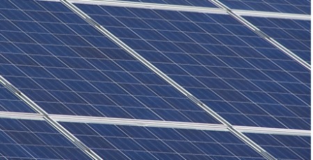
Diamond wire cutting is widely used in wafer dicing for separating individual chips from a wafer, thin wafer processing for advanced 3D IC stacking, and solar cell manufacturing for cutting silicon ingots into wafers.
Conclusão
The diamond cutting wire loop method offers unparalleled advantages in semiconductor wafer cutting, including higher precision, reduced waste, lower stress, and longer tool life. As the demand for thinner and more efficient wafers grows, this technology is set to become the industry standard.
Manufacturers looking to improve yield and reduce costs should consider adopting diamond wire cutting for their wafer dicing processes. With continuous advancements in wire technology, we can expect even greater efficiency and performance in the future.
Would you like to learn more about how diamond wire cutting can optimize your semiconductor production? Let us discuss in the comments!
Perguntas Frequentes
O que é um fio de corte com diamante?
It is a closed loop of high-tensile wire electroplated or resin-bonded with diamond grit, used to slice semiconductor ingots into wafers with very narrow kerf loss.
Última análise: Setembro 2026
Why is kerf loss important in wafer cutting?
Kerf is the silicon removed by the cut itself. Minimizing it means more wafers per ingot, which is the largest cost lever in wafer manufacturing.
Why does diamond wire loop cause less damage than other methods?
It cuts by cold mechanical micro-grinding under coolant, so it introduces neither a heat-affected zone nor high mechanical stress into the wafer.
Key Takeaways
A single-crystal silicon ingot goes through cropping, Moagem de diâmetro, Cortar, Chanframento de borda, lambição e polimento antes de estar pronto.... leia mais
Laço de fio diamantado A tecnologia de corte revolucionou o corte de precisão na fabricação de semicondutores e no processamento de materiais. Este método avançado utiliza impregnado de diamante.... leia mais
Principais Conclusões
O vidro óptico é frágil e sensível a choques térmicos; as fissuras geralmente começam na borda de saída do corte.
Diamante.... leia mais
Principais conclusões
Os wafers de safira são cerca de 0.2 mm de espessura — próximo do diâmetro do fio de diamante — tão grosseiramente 40-50% de... leia mais
Serra de arame diamantado a tecnologia utiliza fios revestidos de diamante para corte preciso e eficiente de materiais. Its significance lies in the... leia mais