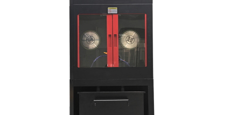
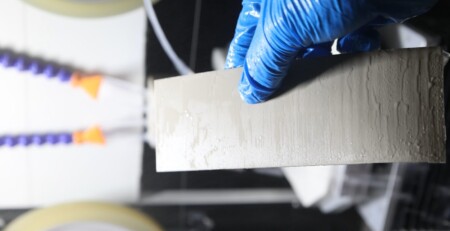
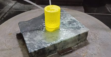
В мире прецизионного производства, немногие процессы так же важны, как нарезка твердых материалов на тонкие пластины, Форменные. Будь то кремний для микросхем, керамические подложки для электроники, или редкоземельные магниты для промышленных применений, процесс распила пластин является основой современной микрообработки.
Резка кремниевых пластин — также называемая пилением кремниевых пластин или просто процессом нарезки пластин — это этап производства, который превращает выращенный монокристаллический слиток в тонкие диски, используемые для чипов и солнечных элементов. Если вы спрашиваете, как режутся кремниевые пластины, краткий ответ: контур из алмазной проволоки, движущийся со скоростью 10–25 м/с, где толщина пластины и полное отклонение толщины (TTV) устанавливаются натяжением проволоки и скоростью подачи. The same physics governs cutting silicon wafers for photovoltaics and for semiconductor substrates; only the thickness target and the tolerance for subsurface damage differ.
But the wafer saw process isn’t a single method. It includes techniques likeПетля из алмазной проволоки режущий, EDM wire cutting, and even compact table top cutter machines for R&D and small-batch production.
Основные выводы
A diamond wire loop cuts silicon with a 100–300 µm steel wire electroplated or resin-bonded with diamond grit, running at 10–25 m/s under continuous coolant.
Diamond wire replaced ID blades and slurry sawing mainly because of kerf loss — a narrower cut means more wafers per ingot, какой является доминирующим фактором стоимости в кремнии.
Три режима дефектов, которые нужно контролировать, это обрыв и износ проводов, микрострещины на поверхности, и изгиб провода, вызванный неравномерным натяжением.
Резка кремниевых пластин, пиление кремниевых пластин и процесс нарезки пластин описывают один и тот же производственный этап: резка кремниевых пластин из монокристаллического слитка алмазной проволокой. Производственные цели обычно составляют 120–250 мкм потерь на пропил при удержании TTV ниже 10 мкм.
– Электроэрозионной резки проволокой в качестве альтернативы для проводящих материалов
– Настольные резательные станки для лабораторного и прототипного использования
Давайте начнем:
1. Что такое пластина?
Прежде чем обсуждать, как нарезают пластины, нам нужно понять, что такое пластина на самом деле.
Пластина — это тонкая, flat disc of semiconductor material — most commonly silicon — on which microelectronic devices are built. Wafers serve as the substrate for integrated circuits (ИС), Солнечные батареи, LEDs, and MEMS (microelectromechanical systems).
– 12 дюймы (300миллиметр) – industry standard today
– 18 дюймы (450миллиметр) – emerging but rare
Thickness is typically between 500–800 microns, but after polishing and backgrinding, finished IC wafers can be as thin as 50–100 microns.
Why Precision Cutting Matters
A single wafer can yield thousands of individual chips (dies). If the cutting process (dicing) is inaccurate, you lose chips, reduce yield, and increase costs. That’s why the wafer saw process must be extremely precise — often within ±1–5 microns.
2. Wafer Saw Process (Петля из алмазной проволоки)
Historically, wafers were cut from ingots using inner-diameter (ID) blades — circular saws with diamond-impregnated rims. But ID blades have limitations:
– Wide kerf (Потери материала)
– Slow cutting speed
– Surface damage
Enter diamond wire sawing.
How Diamond Wire Loop Works
A diamond wire loop consists of a thin steel wire (typically 100–300 microns in diameter) electroplated or resin-bonded with diamond grit. The wire is formed into a continuous loop and driven by pulleys at high speed (10–25 m/s).
По мере движения провода, the diamond grit grinds through the material via a three-body abrasion mechanism. Охлаждающая жидкость (usually deionized water or oil-based fluid) removes debris and heat.
Key Advantages of Diamond Wire Loop for Wafer Sawing
– Gallium arsenide (GaAs) – RF and LED applications
– Sapphire – for LED substrates and watch crystals
– Ceramic substrates – alumina, Циркония
– Quartz and glass – optical and MEMS wafers
3. EDM Wire Cutting (A Complementary Technology)
While diamond wire sawing is excellent for non-conductive and hard materials, EDM wire cutting (Электроэрозионная обработка) offers a completely different mechanism.
What is EDM Wire Cutting?
EDM wire cutting uses a thin, electrically charged brass or copper wire to erode conductive materials through a series of rapid electrical sparks. The wire never touches the workpiece — instead, sparks jump across a small gap, melting and vaporizing tiny particles.
How It Works
Wire electrode (0.05–3 mm diameter) is continuously fed from a spool.
Deionized water acts as a dielectric fluid, flushing away debris and controlling sparks.
CNC controls move the workpiece relative to the wire.
Sparks occur thousands of times per second, gradually cutting through metal.
When to Use EDM Wire Cutting vs. Diamond Wire Sawing
Тип материала
Recommended Method
Кремний, керамический, стекло, сапфир
Петля из алмазной проволоки
Steel, легированный карбид, титан, Inconel
EDM wire cutting
Магнитные материалы (НдФеБ, СмКо)
Both possible; EDM avoids mechanical stress
PCD (polycrystalline diamond)
Электроэрозионная обработка (diamond is conductive if doped)
Advantages of EDM Wire Cutting
No mechanical contact → no stress or burrs
Cuts extremely hard metals (HRC 60+)
Высокая точность (±1–2 microns)
Can cut complex 2D shapes (not just straight slices)
While EDM is rarely used to slice silicon ingots (silicon is only semi-conductive and EDM works poorly on high-resistivity Si), it is used for:
Cutting metalized ceramic substrates
Dicing copper-clad laminates
Slicing tungsten, molybdenum, or Kovar parts used in semiconductor
4. Table Top Cutter Machine
Not every wafer or material cutting job requires a massive industrial saw. For R&D labs, universities, small foundries, and prototype shops, a table top cutter machine is the perfect solution.
Typical Features
Compact footprint (fits on a lab bench)
Adjustable cutting speed and feed rate
Small cutting capacity (typically up to 50–100 mm diameter ingots or blocks)
Integrated coolant system (recirculating or gravity-fed)
Digital readout or CNC control (on high-end models)
Advantages for R&D and Small-Batch Production
Низкая стоимость – всего лишь часть цены промышленных проволочных пил
Быстрая настройка – смена материалов за считанные минуты
Минимальные отходы – идеально для дорогостоящих материалов, таких как GaAs или SiC
1. Понимание монокристаллического кремния
Прежде чем погрузиться в процесс резки, Давайте кратко обсудим монокристаллический кремний и почему для него требуются специальные методы резки.
1.1 Что такое Монокристаллический кремний? ()Вы также можете кликнуть по ссылке, чтобы узнать больше подробностей через Википедию.
Монокристаллический кремний представляет собой высокочистую форму кремния с одним, непрерывная кристаллическая решетчатая структура. Он производится с использованием метода Чохральского (Чехия) или Плавающая зона (ФЗ) метод, в результате получаются цилиндрические слитки.
1.2 Почему прецизионная резка имеет решающее значение
– Полупроводниковая промышленность: Кремниевые пластины должны иметь сверхгладкую поверхность(шероховатость нанометрового уровня) для изготовления микросхем.
– Минимальная потеря пропила: Сокращение отходов материала во время резки повышает экономическую эффективность.
Традиционные методы резки, такие как пилы ID (Пилы с внутренним диаметром) и многопроволочные шлифовальные пилы были заменены пилой с алмазной проволокой благодаря лучшей производительности.
4. Проблемы & Решения в области резки алмазной канатной пилой
Несмотря на свои преимущества, алмазная проволочная пила столкнулась с некоторыми проблемами:
4.1 Обрыв проволоки & Носить
– Причина: Чрезмерное напряжение, абразивный износ, или неисправность охлаждающей жидкости.
– Решение: Мониторинг натяжения в режиме реального времени**, Оптимизированный размер алмазной зернистости, и правильная фильтрация охлаждающей жидкости.
4.2 Поверхностные микротрещины
– Причина: Хрупкий перелом при резке.
– Решение: Контролируемая скорость подачи, Пострезное травление, или отжиг.
4.3 Эффект проволочного лука
– Причина: Неравномерное натяжение проволоки, приводящее к волнистым порезам.
– Решение: Усовершенствованные системы натяжения проволоки с динамическим контролем натяжения.
5.Применение резки алмазной канатной пилой
5.1 Фотоэлектрический (ПВ) Промышленность
– Производство солнечных пластин (Моно PERC, ТОПКОН, HJT-элементы).
– Резка тонких вафель (Менее 150 мкм для высокоэффективных ячеек нового поколения).
5.2 Полупроводниковая промышленность
– Нарезка кремниевых пластин кубиками для производства ИС.
– Усовершенствованная упаковка** (например., Упаковка на уровне пластины).
5.3 Другие области применения
– Резка светодиодной сапфировой подложки.
– Обработка твердых материалов (Так, кварц, керамика).
6.Будущие тенденции в области резки кремниевых пластин
Более тонкие: Спрос на подложки менее 100 мкм стимулирует развитие сверхточных алмазных проволочных пил.
Искусственный интеллект & Автоматизация: Оптимизация процессов на основе машинного обучения для повышения производительности.
Гибридные методы резки: Комбинирование лазерной предварительной биговки + алмазная проволочная пила для ультратонких пластин.
Заключение
Процесс резки пластин является краеугольным камнем современного производства электроники. От выращивания для проводящих материалов, Электроэрозионная резка проволокой предлагает дополнительный бесконтактный метод, способный резать закаленные стали, карбиды, и жаропрочные сплавы с микронной точностью.
And for those working in R&D, prototyping, or small-scale production, a table top cutter machine provides an affordable, flexible entry point into high-precision cutting — without the floor space or budget of an industrial wire saw.
Whether you’re manufacturing 300mm silicon wafers for AI processors or cutting a small alumina substrate on a lab bench, understanding the strengths and limitations of diamond wire loop, Электроэрозионная обработка, and table top cutters will help you select the right tool for the job.a silicon ingot to slicing it into hundreds of thin wafers using a diamond wire loop, every step demands precision, cleanliness, and reliability.
Часто задаваемые вопросы
How are silicon wafers cut from an ingot?
The ingot is grown by the Czochralski or Float Zone method, ground to a precise diameter, then sliced by a diamond wire loop. After sawing, wafer edges are chamfered to prevent chipping, and the wafers are lapped and polished.
What is TTV in wafer cutting?
TTV (total thickness variation) is the difference between the thickest and thinnest points on a wafer. It is the headline metric for wafer sawing quality because downstream lithography needs a flat, uniform surface.
Why did diamond wire replace slurry sawing?
Fixed-diamond wire gives a narrower kerf, a cleaner process with no loose abrasive to manage, и большее количество пластин с одного слитка. Slurry sawing wastes more silicon per cut and carries higher consumable and disposal costs.
What controls breakage when cutting thinner wafers?
Real-time tension monitoring, correctly sized diamond grit, and clean filtered coolant. As wafers drop below 150 мкм, tension stability and feed control matter more than cutting speed.
В чем разница между пилением алмазным проволочным и резкой проволокой EDM для ваферов?
Алмазная проволока режет непроводящие и твёрдые материалы с шириной пропила 120–250 мкм на скорости 2–10 мм/мин и шероховатостью Ra 0,2–0,5 мкм. Резка проволокой EDM работает только с проводящими материалами, но медленнее — 0,5–3 мм/мин, но обеспечивает более тонкую отделку с Ra 0,05–0,2 мкм.
Какой диаметр проволоки используется для резки кремниевых ваферов?
Обычно проволока с металлическим сердечником 100–300 мкм, с нанесённым алмазным зерном в диапазоне 30–100 мкм, наносится методом гальванопокрытия или смолой. Более тонкая проволока уменьшает потери на пропиле, но требует более строгого контроля натяжения.
Насколько тонкими могут быть резаны кремниевые ваферы?
Производственные солнечные вафли обычно 160–180 мкм, следующее поколение элементов движется ниже 150 мкм, и под-100 мкм пластинки являются текущей целью разработки. Каждый следующий шаг требует более тонкой проволоки и более строгого контроля процесса.
Что вызывает изгиб проволоки, и как это исправляется?
Изгиб проволоки — это волнообразный разрез, вызванный неравномерным натяжением проволоки по всей линии реза. Он исправляется с помощью современных систем направляющей проволоки, которые обеспечивают динамическое управление натяжением на протяжении всего разреза.
Технический контент проверен инженерной командой Ensoll — производителя алмазных проволочных петель с 10+ многолетним производственным опытом.
Мы являемся ведущим производителем в Китае, специализирующимся на станках для резки алмазной проволоки. С нашими собственными исследованиями и разработками.. читать далее
Основные выводы
Резка полупроводниковых пластин является критически важным этапом производства интегральных схем, где точность и целостность поверхности определяют выход годных изделий.
Алмазная резка... читать далее
Агат, со своими завораживающими полосами и яркими цветами, является драгоценным камнем, который завораживал ремесленников и коллекционеров на протяжении веков. Однако,... читать далее
Абстрактный: В этой статье представлен тест точного нарезки на PEEK (полиэфирном эфирном кетоне) с использованием а Петля из алмазной проволоки. Тем... читать далее
Петля из алмазной проволоки стали предпочтительным решением для резки твердых, хрупких материалов, таких как ферритовые сердечники, магниты Alnico,... читать далее


 Typical Wafer Sizes
 What is EDM Wire Cutting?
 Монокристаллический кремний представляет собой высокочистую форму кремния с одним, непрерывная кристаллическая решетчатая структура. Он производится с использованием метода Чохральского (Чехия) или Плавающая зона (ФЗ) метод, в результате получаются цилиндрические слитки.