Solar PV Panel Precision Slicing with Diamond Wire Loop: 10 mm Test Data
Sample testing for a European client (Company N) · Ring diamond wire cutting process
Overview
This report documents the precision slicing of solar photovoltaic (PV) panels using a ring diamond wire cutting system. The evaluation covers equipment and wire selection, cutting methodology, process parameters, and the resulting dimensional accuracy, surface quality, and edge integrity of the sliced wafers. Test results indicate that the combination of a gantry-type ring diamond wire machine, water-based cooling, and appropriately matched process parameters delivers stable, high-precision straight slicing of PV panel stock.
1. Test Specimen
| Parameter | Value |
|---|---|
| Material | Solar photovoltaic (PV) panel |
| Hardness | approx. 4–5 Mohs |
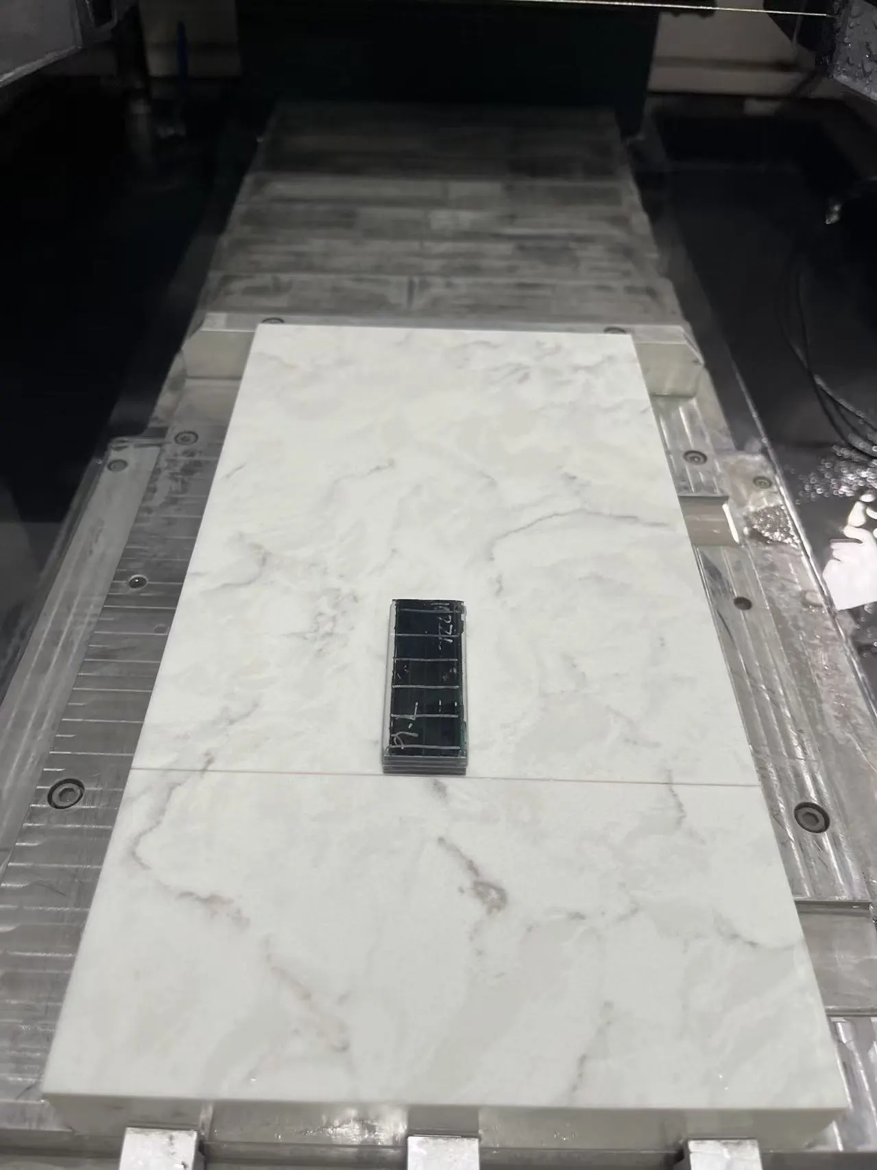
| Workpiece dimensions | 55 mm × 20 mm × 10 mm |
| Target slice thickness | 10 mm |
2. Equipment and Wire Selection
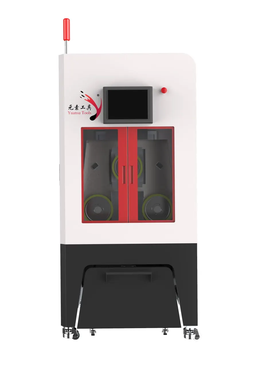
Equipment: ESO-GM. Given the material characteristics of solar PV panels and the requirement for high-precision straight cutting at a 10 mm slice thickness, Ensoll selected the ESO-GM gantry-type ring diamond wire cutting system. The gantry configuration maintains running stability and trajectory accuracy throughout the cut, reducing the influence of machine vibration and fluctuations in cutting load on slice quality.
Coolant: water-based cutting. Water is used as the cooling medium. It cools the contact zone between the diamond wire and the PV panel and carries away part of the heat and debris generated during cutting. This limits localised heat accumulation and debris retention, reduces fluctuation in cutting load, and helps suppress chipping, micro-cracking, and dimensional deviation.
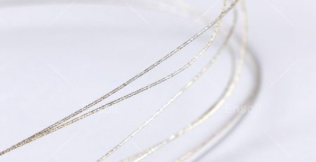
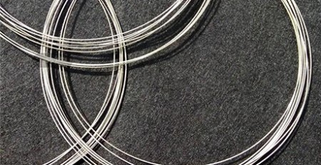
Wire: fully plated. A fully plated diamond wire was selected. The plated construction improves the bonding strength between the diamond abrasive grains and the wire core and provides a more uniform grain distribution. This sustains a continuous and stable material removal rate, reduces grain pull-out and wire wear, and contributes to lower chipping, micro-cracking, and dimensional variation in the sliced PV panels.
3. Cutting Method and Equipment Advantages
Gantry cutting configuration. The gantry structure provides high overall rigidity and running stability. The top-down vertical feed helps maintain a stable wire trajectory and reduces the effect of machine vibration and motion error on cut position and dimensional accuracy. The machine is equipped with a mist-extraction system that promptly removes mist and debris generated during cutting.
Intelligent tension control. The system adjusts diamond wire tension in real time according to cutting conditions and supports both constant-tension and variable-tension modes. This keeps the wire running stably, reduces trajectory deviation and wire breakage caused by tension fluctuation, and limits localised fluctuation in cutting load attributable to unstable wire travel — all of which contribute to better control of slice quality.
Wire-break memory. If the diamond wire breaks or the machine stops abnormally, the system automatically records the current machining position and associated operating state. After the wire is replaced, cutting can resume from the recorded position. This reduces repositioning error and its effect on trajectory and dimensional accuracy, lowers material loss and quality variation from repeated machining, and improves yield.
High-rigidity one-piece cast iron frame. The one-piece cast iron frame increases overall stiffness and vibration resistance, reducing structural vibration and deformation during operation and their effect on wire trajectory, while also damping fluctuation in cutting force. The stable mechanical structure helps prevent uneven local loading of the PV panel during cutting.
4. Process Parameters and Cooling Method
| Parameter | Value |
|---|---|
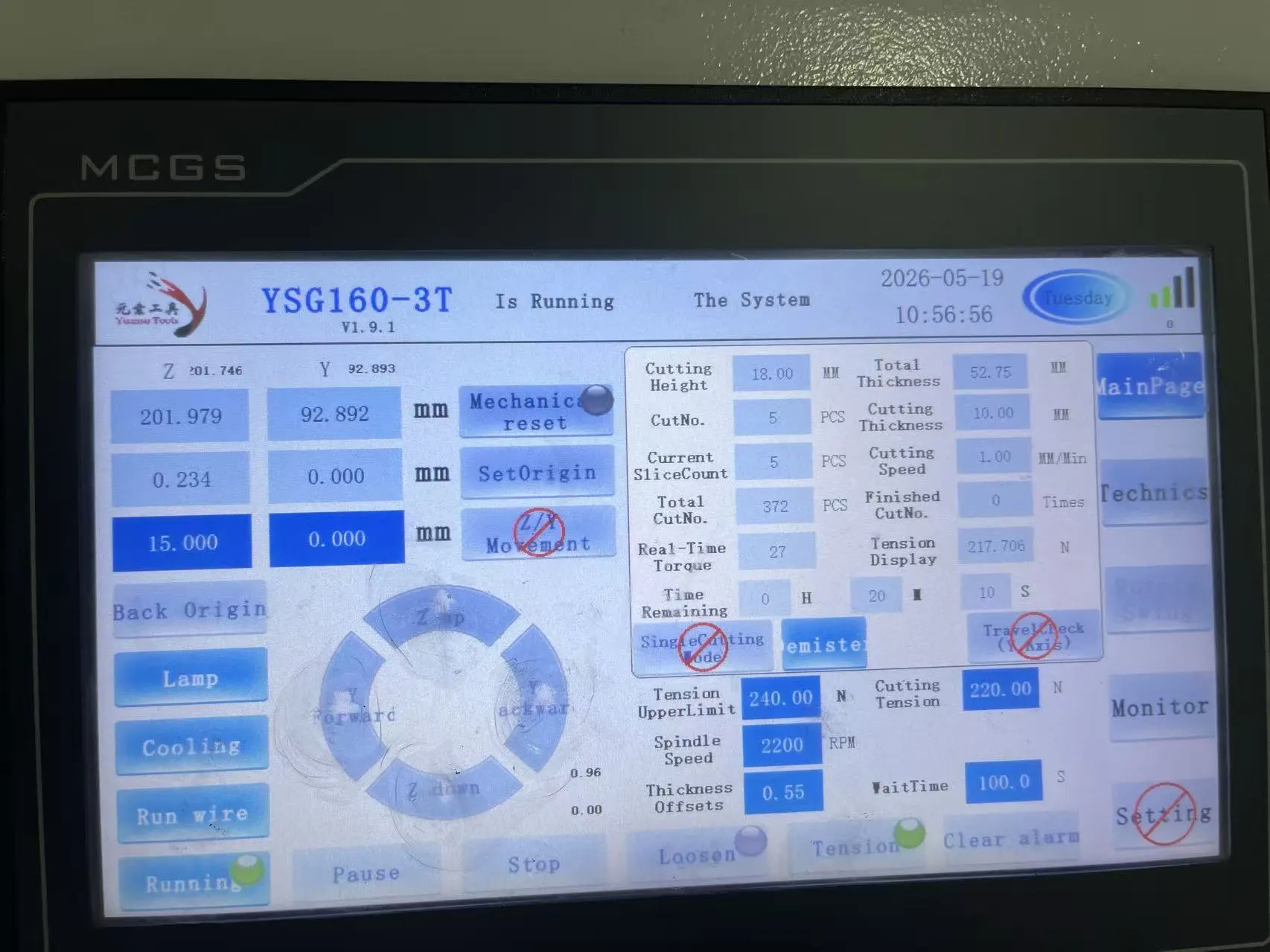
| Wire diameter (mm) | 0.50 × 1930 |
| Wire traverse speed (mm/min) | 20 |
| Cutting width (mm) | 20 |
| Wire tension (N) | 220 |
| Wire speed (m/s) | 26 |
| Wire bow time (s) | 100 |
| Cutting load (N·m) | 27 |
5. Cutting Performance and Results
5.1 TTV Test Data (Unit: mm)
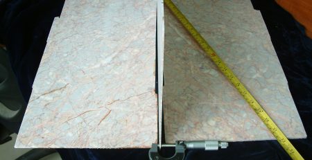
Total Thickness Variation (TTV) was measured using a nine-point grid, dual-probe thickness gauging method on a vacuum-chuck stage. The measurement was applied to PV panel wafers produced by ring diamond wire cutting. The nominal specimen thickness was 10.000 mm.
| Sample | Nine-point thickness readings | Tmax | Tmin | TTV |
|---|---|---|---|---|
| S01 | 9.904, 9.906, 9.908 9.907, 9.909, 9.910 9.908, 9.909, 9.911 |
9.911 | 9.904 | 0.007 |
| S02 | 9.917, 9.919, 9.920 9.918, 9.921, 9.922 9.919, 9.920, 9.923 |
9.923 | 9.917 | 0.006 |
| S03 | 9.932, 9.934, 9.935 9.934, 9.936, 9.937 9.935, 9.936, 9.939 |
9.939 | 9.932 | 0.007 |
| S04 | 9.929, 9.931, 9.932 9.931, 9.934, 9.935 9.932, 9.934, 9.937 |
9.937 | 9.929 | 0.008 |
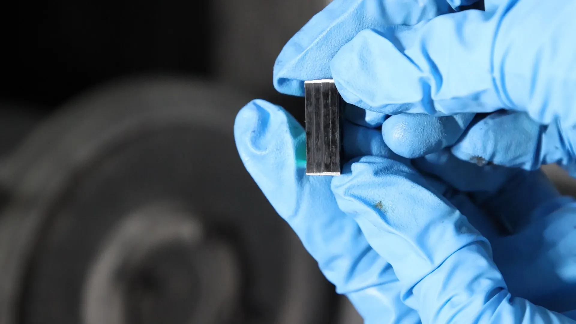
Assessment. Across the four PV panels, measured thicknesses fell within 9.904–9.911 mm (S01), 9.917–9.923 mm (S02), 9.932–9.939 mm (S03), and 9.929–9.937 mm (S04). TTV values ranged from 0.006 mm to 0.008 mm, confirming that the ring diamond wire process holds total thickness variation within a tight band across all four samples.
5.2 Thickness Tolerance Data (Unit: mm)
Thickness tolerance was measured using the same nine-point grid method, with 10.000 mm taken as the nominal thickness of the PV panel wafer. The deviation of each measured point from nominal was calculated, and the maximum positive deviation, maximum negative deviation, and overall thickness deviation range were determined in order to evaluate thickness consistency of the sliced wafers.
| Sample | Mean thickness | Thickness deviation |
|---|---|---|
| S01 | 9.908 | −0.092 |
| S02 | 9.920 | −0.080 |
| S03 | 9.935 | −0.065 |
| S04 | 9.933 | −0.067 |
| Maximum positive deviation | — | −0.065 mm |
| Maximum negative deviation | — | −0.092 mm |
| Thickness tolerance band | — | ±0.014 mm |
Assessment. Against a nominal thickness of 10.000 mm, the four PV panels showed mean thicknesses of 9.908–9.935 mm and thickness deviations of −0.092 to −0.065 mm, all on the negative side. S01 showed the largest deviation and S03 the smallest. The overall thickness tolerance band was ±0.014 mm, indicating good repeatability of slice thickness across the batch.
5.3 Surface Roughness Ra Data (Unit: μm)
Surface roughness (Ra) was measured by stylus profilometry on PV panel wafers after ring diamond wire cutting. Three representative positions — centre, mid-left, and mid-right — were profiled along the cut end face, and the surface roughness parameter Ra was recorded at each position.
| Sample | Ra-1 | Ra-2 | Ra-3 | Mean Ra |
|---|---|---|---|---|
| S01 | 0.72 | 0.81 | 0.76 | 0.76 |
| S02 | 0.65 | 0.71 | 0.68 | 0.68 |
| S03 | 0.58 | 0.64 | 0.61 | 0.61 |
| S04 | 0.69 | 0.77 | 0.73 | 0.73 |
Assessment. Mean Ra across the four samples ranged from 0.61 μm to 0.76 μm, with all individual readings between 0.58 μm and 0.81 μm. The consistency of Ra across the three measurement positions on each wafer indicates a uniform surface finish along the cut face, which is characteristic of stable single-direction ring wire cutting.
5.4 Edge Chipping Data (Unit: μm)
Edge chipping was quantified by optical imaging on a toolmaker’s microscope. The nominal specimen thickness was 10 mm. Specimen edges were cleaned before measurement, and chipping at the cut edge was measured at four positions per sample, with the maximum chipping value recorded.
| Sample | Position 1 | Position 2 | Position 3 | Position 4 | Max. chipping |
|---|---|---|---|---|---|
| S01 | 8.2 | 9.6 | 10.4 | 11.1 | 11.1 |
| S02 | 6.4 | 7.2 | 8.1 | 7.5 | 8.1 |
| S03 | 5.1 | 6.3 | 5.8 | 7.0 | 7.0 |
| S04 | 6.8 | 8.5 | 7.6 | 9.2 | 9.2 |
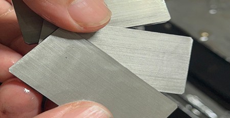
Assessment. Four-point edge inspection of the four PV panel wafers (S01–S04) gave maximum chipping values of 11.1, 8.1, 7.0, and 9.2 μm respectively, with all measurement points falling within 5.1–11.1 μm. S03 showed the smallest maximum chipping (7.0 μm). The results indicate that edge integrity is maintained within a narrow band across the batch.
6. Conclusion
The process control applied in this high-precision slicing trial of solar photovoltaic panels centred on three elements: a purpose-matched cutting machine, water-based cooling, and correctly matched cutting parameters. PV panel stock places specific demands on machine running stability, cutting trajectory, and slice dimensional control, and generates localised stress during cutting that must be managed to preserve edge quality.
Equipment. An ESO-GM ring diamond wire cutting system with a gantry-type cutting structure was used. The gantry configuration provides high overall rigidity and running stability, giving the diamond wire a reliable mechanical basis for continuous travel and trajectory control. Stable machine motion is a prerequisite for consistent slice thickness and surface quality.
Cooling. Water-based cutting was adopted. During cutting the diamond wire remains in continuous contact with the workpiece and removes material by abrasion, generating heat and debris in the cutting zone. Water cooling limits localised temperature rise, carries away part of the debris, and helps suppress thermal damage and chipping at the cut edge.
Process parameters. Wire speed, feed rate, and other key parameters were matched to the machining requirements of PV panel stock and to the target slice thickness. Parameter settings were chosen to maintain stable wire travel and continuous material removal, avoiding excessive feed rates that would raise cutting load and degrade surface finish and edge quality.
Overall. Taken together — slice dimensional accuracy, thickness tolerance, surface roughness (Ra), and cut-edge quality — the coordinated use of a gantry-type purpose-built cutting machine, water-based cooling, and appropriate process parameters provides effective control of high-precision straight slicing of solar photovoltaic panels. This process combination improves dimensional consistency, surface finish, and edge integrity of PV panel wafers, and offers a reliable route for precision slicing of photovoltaic material.