新闻

硅片在光伏行业的繁荣

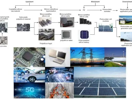
热潮 硅片 in the photovoltaic industry Key Takeaways Carbon-neutrality goals worldwide have made photovoltaics the fastest-growing source of demand for silicon wafers. PV wafer economics are driven by kerf loss and throughput, which is the main reason diamond wire replaced slurry saws across the industry. Larger wafer formats and thinner wafers are the PV industry's structural cost-reduction path, and both raise the bar for cutting precision. Under the background of the carbon neutralization goal and the accelerated application of global clean...
2022 半导体晶圆产业概要

2022 半导体晶圆行业概览 关键要点 半导体硅片是芯片制造的载体基板, and the wafer industry is highly concentrated and technology-intensive. Industry development is driven by larger wafer diameters, tighter flatness specs and growing demand from logic, memory and power devices. 半导体硅晶圆是制造芯片的载体, 也被称为硅片,因为原材料是硅. 经过规划和管理的免硅精炼, 纯化, 单晶硅 生产, 晶圆成型和其他工艺, it can enter...

金刚线硅片切割设备的趋势

1) High line speed and high production capacity support the reduction of single GW investment According to the theory of fracture mechanics and the properties of silicon materials, 当金刚石磨粒的最大切削深度大于硅材料的临界切削深度时, 将发生从塑性切削到脆性断裂切削的转变. 因此, 在金刚石线负载的允许范围内, appropriately increasing the steel wire speed in the multi-wire cutting process is beneficial...

光伏硅片的尺寸变化

关键要点 光伏硅片尺寸是从半导体晶圆规格发展而来的, with PV historically lagging semiconductors in dimension standards. Wafer dimensions keep growing (from 156 mm to 182/210 mm classes) because larger wafers cut module cost per watt. Larger and thinner wafers raise the precision bar for slicing equipment and diamond wire. 光伏硅片的尺寸来源于半导体硅片. 在发展方面 , 光伏落后于半导体 1 自 2 代. 多年来, the size of...

半导体行业的硅锭加工

Key Takeaways In semiconductor wafer preparation, 单晶硅锭被加工成具有高表面精度的裸片,用于光刻. The ingot processing flow includes cropping, 研磨, 切片, 倒角, lapping and polishing, with slicing quality setting downstream workload. 在单晶硅晶圆制备阶段, 硅锭需要加工成具有高表面精度和表面质量的原始硅片或裸硅片,为IC工艺前半段的光刻等工艺的平坦化做准备. Ultra-smooth...