单晶硅片: 现代科技的核心
如果你正在智能手机上阅读此内容, 笔记本电脑, 甚至是专业的工业显示器, you are looking at the direct result of Monocrystalline Silicon (Mono-Si) 科技. Often referred to as the “DNA of the digital age,” monocrystalline silicon wafers are the most critical substrates in the semiconductor and photovoltaic (光伏) industries.
For a practical look at tooling and parameters, our complete guide to 硅片切割 covers wire specification, TTV control and surface finish.
1. What is a Monocrystalline Silicon Wafer?
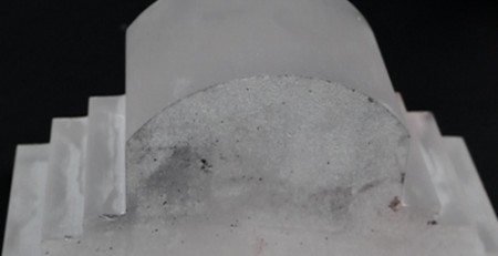
其核心, a Monocrystalline Silicon Wafer is a thin slice of a single, continuous crystal lattice of silicon. Unlike polycrystalline silicon, which consists of many small crystals (grains) oriented in different directions, Mono-Si has a uniform crystal structure throughout the entire material.
 Key Physical Characteristics:
- High Purity: Typically refined to 99.9999999% (9N) or even 11N purity to ensure optimal electron mobility.
- Structural Uniformity: The lack of grain boundaries allows electrons to move freely, making it the most efficient material for conducting electricity in semiconductors.
- Distinct Appearance: Usually dark blue or black, with rounded edges (if cut from a Czochralski ingot) or a perfectly circular shape after precision grinding.
2. 关键功能: 为什么选择单晶硅?
单晶硅晶圆的主要功能是作为半导体衬底.
- 电子迁移率: 由于晶格完整无缺, 不存在 “陷阱” 或晶界来减缓电子运动. 这对于高速微处理器和高能效设备至关重要.
- 热稳定性: 硅在高温下仍能保持机械性能, 这在芯片制造的光刻和蚀刻高温阶段至关重要.
- 光伏效率: 在太阳能领域, 单晶硅晶圆提供最高的能量转换效率 (通常超过 22-24% 在商业组件中) 因为其内部电阻低于多晶硅晶圆.
3. 全球应用领域
单晶硅的多功能性使其能够在多个高增长产业中占据主导地位:
- 集成电路 (集成电路) & 微芯片
从你电脑中的CPU到数据中心的AI加速器, 几乎每一个逻辑芯片最初都是以单晶硅片开始的.
- 太阳能 (光伏) 该市场的硅片生产依赖于 金刚石线环, 其窄切缝决定了每根晶锭可切割出的硅片数量.
随着世界推动实现净零排放 2026, N型单晶硅片已成为高效太阳能电池板的行业标准, 在低光照条件下提供更好的性能并拥有更长的寿命.
- 电力电子 & 电动汽车
现代电动汽车 (电动汽车) 依靠基于硅的功率模块来管理电池放电和电机控制. 尽管碳化硅 (原文如此) 正在崛起, 标准单晶硅仍然是中端功率应用的主力.
4. 工艺挑战: From Ingot to Wafer
The most difficult stage in the life of a silicon wafer is the transition from a heavy, cylindrical ingot to hundreds of wafer-thin slices. This is where the 金刚石绳锯 technology becomes indispensable.
The Problem with Traditional Sawing
Traditional slurry sawing (using loose abrasives) was once the norm. 然而, it was slow, produced massive amounts of toxic waste, and caused significant kerf loss (the silicon material that is turned into useless dust during the cut).
解决方案: The Diamond Wire Saw Cutting Method
在 2026, precision manufacturers like Ensoll have revolutionized this process using the Diamond Wire Saw. This method involves a high-tensile steel wire impregnated with microscopic industrial diamonds.
Why Diamond Wire Sawing is the Industry Standard:
- Extreme Precision: The physical properties of the Diamond Wire Saw enable it to cut through the hard, brittle nature of monocrystalline silicon with micron-level accuracy.
- Eliminating Edge Chipping: One of the biggest hurdles in brittle material processing is “边缘崩裂” (崩边). The gentle grinding action of a diamond wire ensures a smooth, chip-free edge, which is vital for the integrity of the wafer during the later stages of fabrication. The same failure mode dominates 切割氧化铝陶瓷, where exit-edge chipping is the first defect to appear.
- High Efficiency & Throughput: Our endless loop technology allows for linear speeds up to 60m/s, drastically reducing the time required to slice a 12-inch ingot compared to old reciprocating saws.
- iciency & Throughput: Our endless loop technology allows for linear speeds up to 60m/s, drastically reducing the time required to slice a 12-inch ingot compared to old reciprocating saws.
- 低割缝损失: Every micron of silicon saved is a micron of profit. The ultra-thin diameter of the Diamond Wire Saw maximizes the number of wafers obtained from a single ingot.
视频
5. The Manufacturing Flow: A 6-Step Summary
To understand how the Diamond Wire Saw fits into the bigger picture, here is the standard manufacturing flow for a semiconductor-grade wafer:
- Ingot Growth (Czochralski Process): Molten silicon is “pulled” into a single crystal ingot.
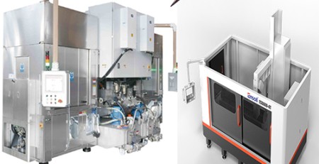
- Slicing (The Diamond Wire Saw Stage): The ingot is sliced into wafers. This is where Ensoll’s Diamond Wire Saw Cutting Machines and loops provide the “精密加工” needed to avoid cracks and minimize waste. A fuller comparison of machine architectures is in our 金刚石绳锯切割机 指南.
- Lapping & 蚀刻: The wafers are thinned and chemical treatments remove any surface damage.
- Polishing: A Chemical Mechanical Polishing (CMP) process creates a mirror-like finish.
- Cleaning: Ultra-pure water and chemicals remove any microscopic particles.
- Inspection: Wafers are checked for TTV (总厚度变化) and crystal defects.
For measured process data on slicing silicon rods with a diamond wire loop (TTV, surface roughness and chipping on a φ330 mm rod), see our latest case study.
- Monocrystalline silicon wafers are the foundation of modern semiconductors and high-efficiency solar cells.
- Diamond wire loop slicing delivers the low-kerf, low-damage cuts these expensive, brittle crystals require.
- Crystal orientation, wire speed, and tension control are the three keys to wafer quality.
结论: Shaping the Future of Technology
Monocrystalline Silicon Wafers are the canvas upon which the future of AI, renewable energy, and global communication is painted. 然而, the quality of that canvas depends entirely on the tools used to create it.
By utilizing the high efficiency, low loss, and high precision of the Diamond Wire Saw, manufacturers can ensure that they are producing the highest grade wafers with the lowest environmental impact. 在 Ensoll, we provide the integrated machine and wire solutions that make this precision possible.
常见问题
What is a monocrystalline silicon wafer?
A thin slice cut from a single continuous silicon crystal. Its uniform crystal lattice delivers the electronic performance required by semiconductors and high-efficiency solar cells.
Why are diamond wire loops used to slice monocrystalline silicon?
The material is hard, brittle, and expensive. The loop’s narrow kerf and low cutting force minimize material loss and sub-surface damage, directly improving yield.
What quality metrics matter for silicon wafers?
The three standard indicators are total thickness variation (TTV), 表面粗糙度 (Ra), and edge chipping.
What size silicon rods can a diamond wire loop slice?
Production diamond wire loop machines handle everything from small R&D ingots up to φ330 mm rods and beyond.
技术内容由Ensoll工程团队审核——一家金刚线环制造商 10+ 多年生产经验.