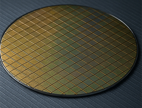
Il taglio dei wafer semiconduttori è una fase critica nella produzione di circuiti integrati dove la precisione e l'integrità della superficie determinano la resa del dispositivo.
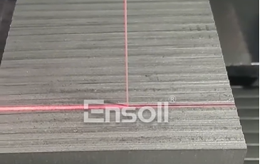
Un filo diamantato da taglio a loop è un filo rivestito di diamante ad anello chiuso che affetta i lingotti con estrema precisione, minima perdita di filetto.
I suoi principali vantaggi sono stress termici e meccanici inferiori rispetto al taglio laser o a lama, cosa che è particolarmente importante man mano che i wafer diventano più sottili.
Semiconduttore il taglio dei wafer è un processo critico nella produzione di circuiti integrati (Ics) e altri dispositivi microelettronici. Precisione ed efficienza sono fondamentali, poiché anche piccoli difetti possono portare a significativi problemi di prestazioni nel prodotto finale. Tra le varie tecnologie di taglio disponibili, L'anello di filo da taglio diamantato è emerso come un metodo superiore grazie alla sua eccezionale precisione, Minima perdita di materiale, e maggiore durata utensile.
In questo articolo, esploreremo perché taglio a filo diamantato sta diventando la scelta preferita per il taglio dei wafer semiconduttori e come supera i metodi tradizionali come il taglio a lama e il taglio laser.
Le sfide del taglio dei wafer semiconduttori
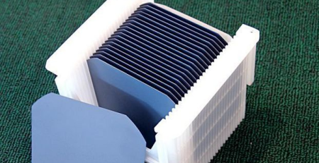
I wafer semiconduttori, tipicamente realizzati in silicio, sono estremamente sottili e fragili. Il processo di taglio deve garantire un'alta precisione con una larghezza del solco minima e senza scheggiature, bassi danni termici per prevenire microcrepe, e un alto rendimento per una produzione economica.
I metodi tradizionali come il taglio meccanico con lama possono causare microcrepe e perdita di materiale, mentre il taglio laser può introdurre stress termico. Qui è dove eccelle la tecnologia del filo da taglio diamantato a loop.
Cos'è il filo da taglio diamantato a loop?
Un filo da taglio diamantato a loop è un filo sottile, flessibile, incorporato con particelle abrasive di diamante. Funziona muovendo continuamente il filo sulla wafer, per consentire tagli precisi e lisci con uno stress meccanico minimo. .
Vantaggi principali del taglio con filo diamantato
Taglio ultra-preciso con perdita minima di solco
Il taglio con filo diamantato produce un solco estremamente stretto, fino a 20-30 µm, consentendo una maggiore resa dei wafer rispetto alla segagione a lama. L'azione abrasiva fine riduce scheggiature e difetti sui bordi, cruciale per wafer delicati.
Riduzione dello Spreco di Materiale
Poiché il filo è molto più sottile di una lama da sega, si spreca meno silicio, migliorando l'utilizzo del materiale e riducendo i costi di produzione.
Minore Stress Termico e Meccanico
A differenza del taglio laser, il taglio con filo diamantato genera calore minimo, prevenendo danni termici al wafer. Il processo applica pressione uniforme, riducendo il rischio di microfessure.
Maggiore durata dell'utensile e minor manutenzione
Il diamante è uno dei materiali più duri, garantendo durata e prestazioni costanti per un uso prolungato. A differenza delle lame che si consumano rapidamente, il filo diamantato mantiene l'affilatura più a lungo, riducendo i tempi di fermo per le sostituzioni.
Versatilità nel taglio di vari materiali
Oltre a wafer di silicio, diamond wire loops can cut gallium arsenide (GaAs), zaffiro, and ceramic substrates with high precision.
Applications in Semiconductor Manufacturing
Diamond wire cutting is widely used in wafer dicing for separating individual chips from a wafer, thin wafer processing for advanced 3D IC stacking, and solar cell manufacturing for cutting silicon ingots into wafers.
Conclusione
The diamond cutting wire loop method offers unparalleled advantages in semiconductor wafer cutting, including higher precision, reduced waste, lower stress, and longer tool life. As the demand for thinner and more efficient wafers grows, this technology is set to become the industry standard.
Manufacturers looking to improve yield and reduce costs should consider adopting diamond wire cutting for their wafer dicing processes. With continuous advancements in wire technology, possiamo aspettarci un'efficienza e prestazioni ancora maggiori in futuro.
Vorresti saperne di più su come il taglio con filo diamantato può ottimizzare la tua produzione di semiconduttori? Discutiamone nei commenti!
Domande Frequenti
Cos'è un filo di taglio diamantato a loop?
È un anello chiuso di filo ad alta resistenza elettrodeposto o legato con resina con grana di diamante, utilizzato per affettare lingotti di semiconduttore in wafer con perdita di kerf molto ridotta.
Ultima revisione: Settembre 2026
Perché la perdita di kerf è importante nel taglio dei wafer?
Il kerf è il silicio rimosso dal taglio stesso. Minimizzarlo significa più wafer per lingotto, che è la principale leva di costo nella produzione di wafer.
Perché il filo diamantato a loop causa meno danni rispetto ad altri metodi?
Taglia tramite micro-macinatura meccanica a freddo sotto raffreddamento, quindi non introduce né una zona interessata dal calore né un alto stress meccanico nel wafer.
Punti chiave
Il vetro ottico è fragile e sensibile agli shock termici; le crepe di solito iniziano al bordo di uscita del taglio.
Diamante... leggi di più
Key Takeaways
Rubber blocks embedded with metal wires (such as tire-derived blocks) are extremely difficult to cut with conventional blades because... leggi di più
Il silicio monocristallino è il fondamento delle moderne industrie dei semiconduttori e del fotovoltaico. Per trasformare i lingotti di silicio in wafer funzionali, taglio di precisione... leggi di più
Agata, con le sue affascinanti venature e i colori vivaci, è una gemma che ha catturato l'attenzione di artigiani e collezionisti per secoli. Tuttavia,... leggi di più
Punti chiave
I produttori di PV hanno bisogno di più wafer per lingotto a costi sempre più bassi — esattamente ciò che offre la segatura con filo di diamante.
Stretto... leggi di più
Principali punti chiave
SiC e GaN sono semiconduttori di terza generazione che stanno trasformando l'elettronica di potenza, 5G e veicoli elettrici — ma sono estremamente difficili da... leggi di più
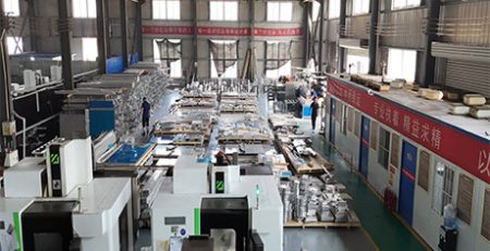
In qualità di produttore leader mondiale di utensili e attrezzature industriali, La nostra azienda è molto orgogliosa dei nostri impianti di produzione all'avanguardia.. leggi di più
Punti chiave
Il vetro ottico è prodotto da una composizione precisa di silicati e ossidi metallici per alta trasparenza e minima dispersione della luce... leggi di più