Nel mondo della produzione di precisione, few processes are as critical as slicing hard materials into thin, uniform wafers. Che si tratti di silicio per microchip, substrati in ceramica per l'elettronica, o magneti di terre rare per applicazioni industriali, il processo di taglio delle wafer è la spina dorsale della microfabbricazione moderna.
La fettilatura del wafer di silicio — chiamata anche segatura dei wafer di silicio o semplicemente processo di taglio del wafer — è la fase di produzione che trasforma un lingotto monocristallino cresciuto nei sottili dischi utilizzati per chip e celle solari. Se ti stai chiedendo come vengono tagliate le wafer di silicio, la risposta breve è un filo di diamante che scorre a 10–25 m/s, dove lo spessore della wafer e la variazione totale dello spessore (TTV) sono determinati dalla tensione del filo e dalla velocità di avanzamento. La stessa fisica governa il taglio delle wafer di silicio per il fotovoltaico e per i substrati dei semiconduttori; solo l'obiettivo di spessore e la tolleranza per il danno sottosuperficiale differiscono.
Ma il processo di taglio delle wafer non è un singolo metodo. Include tecniche come anello di filo diamantato taglio, taglio a filo EDM, e persino macchine compatte da tavolo per R&D e produzione in piccoli lotti.
Punti Chiave
Un anello di filo diamantato taglia silicio con filo d'acciaio da 100–300 μm elettroplaccato o legato in resina con grana diamantata, che funziona a 10–25 m/s sotto refrigerante continuo.
Risultati tipici del taglio: 120taglio superficiale da 250 μm, Ra 0,2–0,5 μm finitura superficiale, 2velocità di taglio di 10 mm/min.
Filo diamantato sostituito lame di identificazione e segatura a foglia principalmente a causa della perdita di taglio — un taglio più stretto significa più wafer per lingotto, che è la leva di costo dominante nel silicio.
i tre modi di difetto da controllare sono: rottura e usura del filo, micro-crepe superficiali, arco del filo causato da tensione irregolare.
taglio del wafer di silicio, segatura di wafer in silicio e il processo di taglio del wafer descrivono tutti lo stesso passaggio di produzione: taglio di wafer di silicio da lingotti monocristallini con filo diamantato. Production targets are typically 120–250 µm kerf loss with TTV held under 10 µm.
– EDM wire cutting as an alternative for conductive materials
– Table top cutter machines for laboratory and prototyping use
Immergiamoci:
1. What is a Wafer?
Before discussing how wafers are cut, we need to understand what a wafer actually is.
A wafer is a thin, flat disc of semiconductor material — most commonly silicon — on which microelectronic devices are built. Wafers serve as the substrate for integrated circuits (Ics), celle solari, LEDs, and MEMS (microelectromechanical systems).
– 12 Pollici (300millimetro) – industry standard today
– 18 Pollici (450millimetro) – emerging but rare
Thickness is typically between 500–800 microns, but after polishing and backgrinding, finished IC wafers can be as thin as 50–100 microns.
Why Precision Cutting Matters
A single wafer can yield thousands of individual chips (dies). If the cutting process (dicing) is inaccurate, you lose chips, reduce yield, and increase costs. That’s why the wafer saw process must be extremely precise — often within ±1–5 microns.
Historically, wafers were cut from ingots using inner-diameter (DI) blades — circular saws with diamond-impregnated rims. But ID blades have limitations:
– Wide kerf (perdita di materiale)
– Slow cutting speed
– Surface damage
Enter diamond wire sawing.
How Diamond Wire Loop Works
Un filo di diamante consiste in un sottile filo d'acciaio (tipicamente 100–300 micron di diametro) placcato elettroliticamente o legato con resina con granuli di diamante. Il filo viene formato in un anello continuo e mosso da pulegge ad alta velocità (10–25 m/s).
Mentre il filo si muove, i granuli di diamante macinano il materiale tramite un meccanismo di abrasione a tre corpi. Refrigerante (di solito acqua deionizzata o fluido a base di olio) rimuove detriti e calore.
Principali vantaggi del filo di diamante per il taglio di wafer
Criterio
Anello di filo diamantato
Taglio a filo EDM
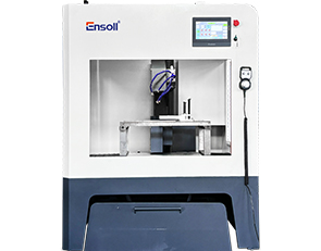
Taglierina da tavolo (Filo diamantato)
Tipo di materiale
Non conduttivo & duro
Solo conduttivo
Uguale al filo di diamante
Kerf tipico
120–250 µm
50–150 µm
150–300 µm
Finitura della superficie
Buono (Ra 0,2–0,5 µm)
Eccellente (Ra 0,05–0,2 µm)
Buono (Ra 0,3–0,6 µm)
Velocità di taglio
Veloce (2–10 mm/min)
Lento (0.5–3 mm/min)
Moderato (1–5 mm/min)
Costo dell'attrezzatura
Alta (industriale) / Media (da tavolo)
Da medio ad alto
Da basso a medio
Migliore per
Wafer di silicio, ceramica, zaffiro
Acciaio per utensili, carburo, titanio
R&D, piccoli lingotti, materiali fragili
Processo Passo-Passo di Taglio dei Wafer (Dalla Lingottiera al Wafer)
1.Crescita del Lingotto – Il lingotto di silicio monocristallino viene cresciuto tramite metodo Czochralski o Float Zone.
Rettifica – Il lingotto viene rettificato a diametro preciso.
Taglio a Filo – Il filo diamantato a loop taglia il lingotto in wafer individuali.
Smussatura dei Bordi – I bordi dei wafer vengono smussati per prevenire scheggiature.
Lappatura – Rimuove i segni del taglio e appiana il wafer.
Incisione – Rimuove lo strato superficiale danneggiato.
Lucidatura – Crea una superficie speculare per la litografia.
Applicazioni Oltre il Silicio
Il taglio con filo diamantato non è solo per wafer di silicio. È anche utilizzato per:
– Carburo di silicio (Sic) – semiconduttori a bandgap largo
– Arseniuro di gallio (GaAs) – applicazioni RF e LED
– Zaffiro – per substrati LED e cristalli per orologi
– Substrati ceramici – allumina, zirconia
– Quarzo e vetro – wafer ottici e MEMS
3. Taglio a filo EDM (Una tecnologia complementare)
Mentre il taglio con filo di diamante è eccellente per materiali non conduttivi e duri, taglio a filo EDM (Lavorazione a scarica elettrica) offre un meccanismo completamente diverso.
Cos'è il taglio EDM a filo?
Il taglio EDM a filo utilizza un sottile, filo di ottone o rame caricato elettricamente per erodere materiali conduttivi attraverso una serie di rapidi impulsi elettrici. Il filo non tocca mai il pezzo — invece, gli impulsi saltano attraverso un piccolo intervallo, fondendo e vaporizzando minuscole particelle.
Come funziona
Elettrodo a filo (0.05– diametro 3 mm) viene continuamente alimentato da una bobina.
L'acqua deionizzata funge da fluido dielettrico, asportando i detriti e controllando gli impulsi.
I controlli CNC muovono il pezzo rispetto al filo.
Gli impulsi si verificano migliaia di volte al secondo, taglio graduale del metallo.
Quando utilizzare il taglio a filo EDM vs. Segatrice a filo diamantato
Tipo di materiale
Metodo consigliato
Silicio, ceramico, vetro, zaffiro
Anello di filo diamantato
Acciaio, carburo, titanio, Inconel
taglio a filo EDM
Materiali magnetici (NdFeB, SmCo)
Entrambi possibili; L'EDM evita lo stress meccanico
PCD (diamante policristallino)
EDM (il diamante è conduttivo se drogato)
Vantaggi del taglio a filo EDM
Nessun contatto meccanico → nessuno stress o sbavature
Taglia metalli estremamente duri (HRC 60+)
Alta precisione (±1–2 micron)
Può tagliare forme 2D complesse (non solo fette dritte)
Limitazioni
Velocità di taglio lenta rispetto alla sega a filo
Funziona solo su materiali conduttivi
Costo operativo più elevato (filo, filtri, fluido dielettrico)
Sebbene l'EDM sia raramente usato per affettare lingotti di silicio (il silicio è solo semiconduttivo e l'EDM funziona male su Si ad alta resistività), è utilizzato per:
Taglio di substrati ceramici metallizzati
Taglio di laminati rivestiti di rame
Affettare tungsteno, molibdeno, o parti Kovar utilizzate nel settore dei semiconduttori
4. Macchina taglierina da tavolo
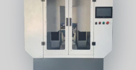
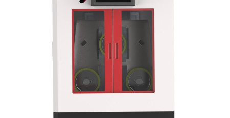
Not every wafer or material cutting job requires a massive industrial saw. For R&D labs, universities, small foundries, and prototype shops, a table top cutter machine is the perfect solution.
Typical Features
Compact footprint (fits on a lab bench)
Adjustable cutting speed and feed rate
Small cutting capacity (typically up to 50–100 mm diameter ingots or blocks)
Integrated coolant system (recirculating or gravity-fed)
Digital readout or CNC control (on high-end models)
Minimal waste – ideal for expensive materials like GaAs or SiC
1. Comprendere il silicio monocristallino
Prima di entrare nel processo di taglio, discutiamo brevemente il silicio monocristallino e il motivo per cui richiede tecniche di taglio specializzate.
1.1 Cos'è Silicio monocristallino? (Puoi anche cliccare sul link per saperne di più tramite Wikipedia.)
Il silicio monocristallino è una forma altamente pura di silicio con una singola, struttura cristallina continua. It is produced using the Czochralski (CZ) method or the Float Zone (FZ) method, resulting in cylindrical ingots.
1.2 Perché il taglio di precisione è cruciale
– Industria dei semiconduttori: I wafer di silicio devono avere superfici ultra lisce(rugosità a livello nanometrico) per la fabbricazione di microchip.
-Industria fotovoltaica: Le celle solari richiedono spessori sottili, uniform wafers(tipicamente 160-180µm) per massimizzare l'efficienza.
– Perdita di Scanalatura Minima: Ridurre gli sprechi di materiale durante il taglio migliora l'efficienza dei costi.
I metodi di taglio tradizionali come le seghe a diametro interno (sega a diametro interno) e le seghe a filo multiplo con pasta abrasiva sono stati sostituiti dal taglio con seghe a filo diamantato grazie alle prestazioni superiori.
4. Sfide & Soluzioni nel taglio con sega a filo diamantato
Nonostante i suoi vantaggi, Sega a filo diamantato affronta alcune sfide:
4.1 Rottura del filo & Usura
– Causa: Tensione eccessiva, usura abrasiva, o guasto del refrigerante.
– Soluzione: Monitoraggio della tensione in tempo reale**, dimensione ottimizzata della grana di diamante, e filtrazione adeguata del refrigerante.
4.2 Microfessure superficiali
– Causa: Frattura fragile durante il taglio.
– Soluzione: Velocità di avanzamento controllata, incisione post-taglio, o ricottura.
4.3 Effetto curvatura del filo
– Causa: Tensione non uniforme del filo che porta a tagli ondulati.
– Soluzione: Sistemi avanzati di guida del filo con controllo dinamico della tensione.
5.Applicazioni del taglio con sega a filo diamantato
5.1 Fotovoltaico (PV) Industria
– Produzione di wafer solari (Mono PERC, TOPCon, celle HJT).
– Taglio di wafer sottili (sotto 150 µm per celle ad alta efficienza di prossima generazione).
5.2 Industria dei semiconduttori
– Taglio di wafer di silicio per la produzione di IC.
– Packaging avanzato** (ad es., packaging a livello di wafer).
5.3 Altre applicazioni
– Taglio di substrati LED in zaffiro.
– Lavorazione di materiali duri (Sic, quarzo, ceramica).
6.Tendenze future nel taglio dei wafer di silicio
Wafer più sottili: La domanda di wafer sotto i 100µm spinge i progressi nel taglio ultra-preciso con sega a filo diamantato.
IA & Automazione: Ottimizzazione dei processi basata sull'apprendimento automatico per una resa più alta.
Metodi di taglio ibridi: Combinazione di pre-scoratura laser + saw a filo diamantato per wafer ultra-sottili.
Conclusione
Il processo di segatura dei wafer è una pietra miliare della produzione elettronica moderna. Dalla crescita dei materiali conduttivi, Il taglio con filo EDM offre un metodo complementare senza contatto in grado di tagliare acciai temprati, carburi, e superleghe con precisione a livello micronico.
E per chi lavora in R&D, prototipazione, o produzione su piccola scala, una macchina da tavolo per il taglio offre un punto di ingresso conveniente, flessibile nel taglio ad alta precisione — senza lo spazio a pavimento o il budget di una sega a filo industriale.
Che tu stia producendo wafer di silicio da 300 mm per processori AI o tagliando un piccolo substrato di allumina su un banco di laboratorio, comprendere i punti di forza e i limiti della filo diamantato a loop, EDM, e dei cutter da tavolo ti aiuterà a selezionare lo strumento giusto per il lavoro. Da un lingotto di silicio a fette centinaia di wafer sottili usando un filo diamantato a loop, ogni passo richiede precisione, pulizia, e affidabilità.
Domande Frequenti
Come vengono ricavati i wafer di silicio da un lingotto?
Il lingotto viene coltivato con il metodo Czochralski o Float Zone, levigato a un diametro preciso, poi tagliato con un filo diamantato a loop. Dopo il taglio, i bordi del wafer vengono smussati per prevenire scheggiature, e i wafer vengono levigati e lucidati.
Cos'è il TTV nel taglio dei wafer?
TTV (variazione dello spessore totale) è la differenza tra i punti più spessi e più sottili di un wafer. È la misura principale della qualità della segagione dei wafer perché la litografia a valle necessita di una superficie piatta, uniforme.
Perché il filo diamantato ha sostituito il taglio con sospensione abrasiva?
Il filo diamantato fisso offre un solco più stretto, un processo più pulito senza abrasivi sciolti da gestire, e più wafer per lingotto. La segagione a sospensione di abrasivo spreca più silicio per taglio e comporta costi maggiori di consumabili e smaltimento.
Cosa controlla la rottura quando si tagliano wafer più sottili?
Monitoraggio della tensione in tempo reale, granulometria del diamante correttamente dimensionata, e refrigerante pulito e filtrato. Quando i wafer scendono al di sotto di 150 µm, la stabilità della tensione e il controllo dell’alimentazione contano più della velocità di taglio.
Qual è la differenza tra la segagione a filo diamantato e il taglio a filo EDM per i wafer?
Diamond wire cuts non-conductive and hard materials with a 120–250 µm kerf at 2–10 mm/min and Ra 0.2–0.5 µm. EDM wire cutting only works on conductive materials, is slower at 0.5–3 mm/min, but produces a finer finish of Ra 0.05–0.2 µm.
What wire diameter is used for silicon wafer cutting?
Typically 100–300 µm steel core wire, carrying diamond grit in the 30–100 µm range, applied by electroplating or resin bonding. Thinner wire reduces kerf loss but needs tighter tension control.
How thin can silicon wafers be cut?
Production solar wafers are commonly 160–180 µm, next-generation cells are moving below 150 µm, and sub-100 µm wafers are the current development target. Each step down demands finer wire and tighter process control.
Cosa causa l'arco del filo, e come si corregge?
L'arco del filo è un taglio ondulato causato da una tensione irregolare del filo durante il taglio. Si corregge con sistemi avanzati di guida del filo che applicano il controllo dinamico della tensione durante tutto il taglio.
Contenuto tecnico esaminato dal team di ingegneria Ensoll — un produttore di anelli diamantati con 10+ anni di esperienza produttiva.
Punti chiave
Il taglio a filo EDM taglia materiali elettricamente conduttivi utilizzando erosione a scintilla, quindi la durezza del materiale è irrilevante - anche acciaio per utensili indurito... leggi di più
Punti chiave
Un lingotto di silicio monocristallino passa attraverso il taglio, levigatura del diametro, tagliatura, smussamento dei bordi, levigatura e lucidatura prima di essere pronto... leggi di più
Punti chiave
Esistono quattro principali tipi di macchine a sega a filo diamantato: filo continuo, multi-filo, filo fisso e macchine portatili.
Segatrice a filo continuo... leggi di più
Key Takeaways
Diamond wire cutting has demonstrated precision down to 1mm in real cutting cases, rendendolo un metodo di riferimento per... leggi di più
Astratto: Questo articolo presenta un test di affettamento di precisione sul PEEK (polieter etere chetone) utilizzando una anello di filo diamantato. Le... leggi di più
Astratto: Questo foglio di riferimento elenca la finestra di processo convalidata nel PMI di Ensoll
(polimetacrilimmide) test di taglio della schiuma strutturale su un orizzontale ESH600-4T
leggi di più
Astratto: Questo rapporto applicativo documenta un test di taglio diritto ad alta precisione su un foglio di vetro BG38 fornito da un cliente europeo. The workpiece measured... leggi di più
Key Takeaways
NdFeB magnets are built from three elements with distinct roles: il neodimio fornisce la forza magnetica, il ferro stabilizza la struttura... leggi di più

 Typical Wafer Sizes
 Cos'è il taglio EDM a filo?
 Il silicio monocristallino è una forma altamente pura di silicio con una singola, struttura cristallina continua. It is produced using the Czochralski (CZ) method or the Float Zone (FZ) method, resulting in cylindrical ingots.