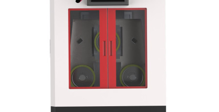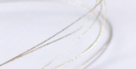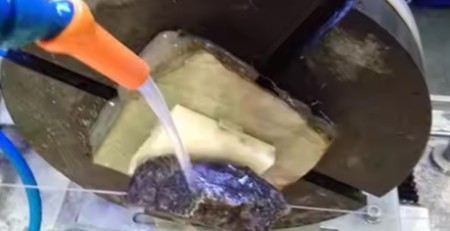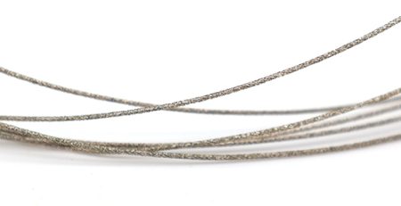
PV半導体における無限ダイヤモンドワイヤーループソー
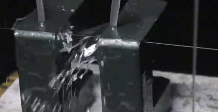
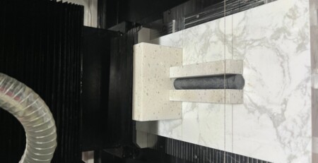
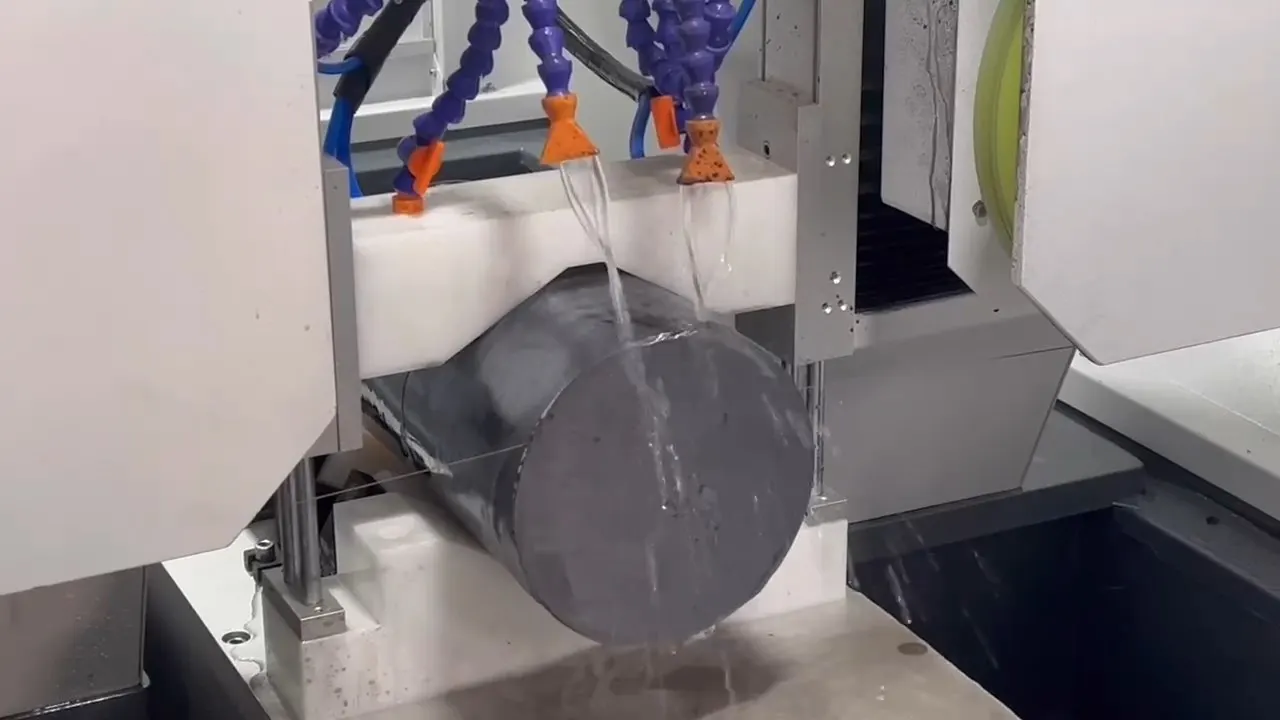
- Diamond wire loop cutting has become a key process in silicon wafer production for both photovoltaics and semiconductors.
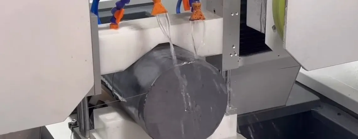
- A continuous loop running at high speed with diamond abrasive delivers consistent, low-damage slicing at production throughput.
進化し続ける半導体製造の現場で, 精度と効率が最重要. この最先端のイノベーション, known as diamond wire loop cutting, has played a key role in the production of silicon wafers, enabling semiconductor manufacturers to achieve unmatched precision and productivity.
Endless Diamond wire loop cutting technology is an innovative method used in semiconductor manufacturing to improve the precision and efficiency of silicon cutting. This technology has been widely used in silicon wafer production in recent years, because it can reduce the loss of silicon wafers, improve cutting quality, and reduce production costs.
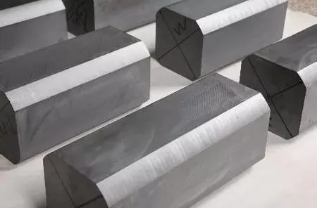
さらに, diamond wire loop cutting technology can also cut thinner slices on silicon wafers, thereby reducing material waste. The advent of diamond wire loop cutting technology has improved the quality and precision of silicon wafers.
よくある質問
What role does diamond wire loop cutting play in semiconductor manufacturing?
It slices silicon ingots into wafers with high precision and low damage, setting the quality foundation for every later fabrication step.
What does “endless” mean in a diamond wire saw?
Endless means the wire forms a closed loop that runs continuously in one direction, unlike long-wire systems that spool back and forth.
What are the advantages of diamond wire loop sawing for PV wafers?
Narrow kerf loss, high throughput and low wafer breakage — the three factors that dominate PV wafer cost.
Technical content reviewed by the Ensoll engineering team — a diamond wire loop manufacturer with 10+ years of production experience.