Thin-Film Solar Cutting: Diamond Wire Loop Excels
- Thin-film PV materials such as CdTe, CIGSやa-Siは、熱的および機械的な損傷の両方を避ける精密な切断が必要です.
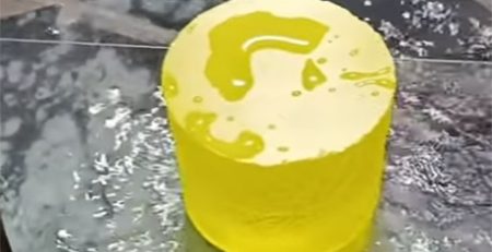
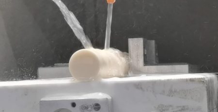
- Diamond wire loop outperforms lasers and blades on brittle thin-film stacks: it is a cold, narrow-kerf process with clean edges.
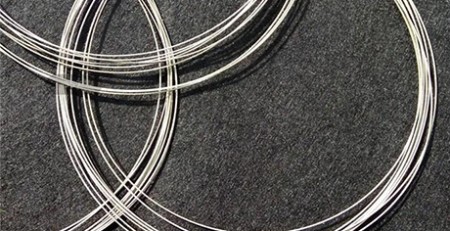
- Diamond wire loop cutting is applied in CdTe modules, CIGS and amorphous silicon panels, and is positioned as the future of advanced PV cutting.
The solar energy industry continues to evolve with advanced thin-film photovoltaic (PV) technologies offering higher efficiency and lower production costs. これらのうち, Cadmium Telluride (CdTe), Copper Indium Gallium Selenide (CIGS), and Amorphous Silicon (a-Si) stand out as key materials for next-generation solar panels.
しかし, manufacturing high-performance thin-film solar cells requires precision cutting to minimize material waste and maintain structural integrity. While various cutting methods exist, ダイヤモンドカッティングワイヤーループ technology has emerged as the most efficient solution for thin-film semiconductors.
 このブログでは、以下を探ります:
✔ Why thin-film solar materials need precision cutting
✔ Comparison of cutting technologies
✔ Why diamond cutting wire loop is the best choice
✔ Industry applications and future trends
Thin-film stock fails for the same reason thin wafers do — see the yield notes under the wafer cutting process.
Why Thin-Film Solar Materials Require Precision Cutting
Thin-film solar cells are significantly thinner (1–4 µm) than traditional シリコンウエハ, making them more challenging to cut without damage. Key challenges include:
- Minimal Kerf Loss Requirement
– Thin-film materials are expensive; waste reduction is critical for cost efficiency.
– Traditional saws create >200 µm kerf loss, while diamond wire loops achieve <100 µm.
- High-Quality Edge Finish Needed
– Rough edges reduce cell efficiency due to increased recombination losses.
– Laser cutting can cause heat damage, degrading performance.
- Scalability for Mass Production
– Thin-film solar manufacturing requires high-throughput cutting without sacrificing quality.
Cutting Technologies for Thin-Film Solar Materials
| Method | Pros | Cons | Best For |
| Mechanical Scribing | Low cost | High breakage rate | Lab-scale R&D |
| レーザー切断 | 高精度 | Heat-affected zone (ハズ) | Small-scale production |
| Ultrasonic Cutting | Minimal stress | Slow processing speed | Flexible substrates |
| ダイヤモンドカッティングワイヤーループ | No HAZ, 高速, low kerf loss | Higher initial investment | Mass production |
Why Diamond Cutting Wire Loop Outperforms Other Methods
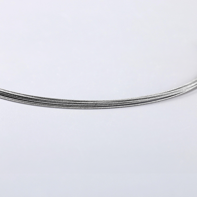
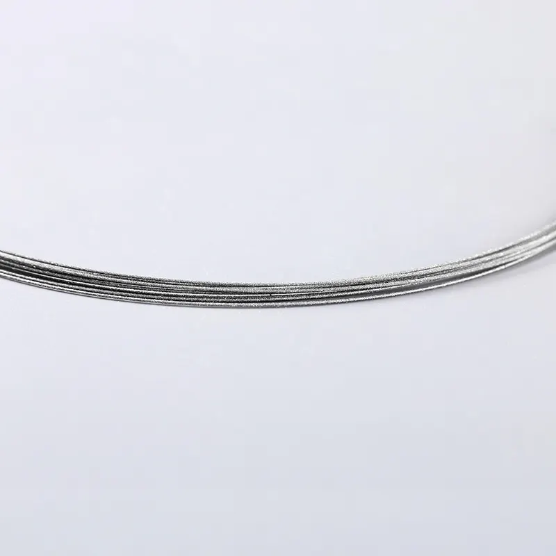
– Achieves 50–80 µm kerf width, preserving more active material.
– 30% higher material yield vs. laser/mechanical methods.
- 冷間切断プロセス (No Heat Damage)
– Unlike lasers, diamond wire loops do not generate heat, preventing:
– Thermal stress cracks in CdTe
– Layer delamination in CIGS & a-Si
3. Superior Edge Quality
– Surface roughness <0.5 µm (vs. 2–5 µm with lasers).
– Smoother edges = higher cell efficiency (up to 1.5% gain).
4. High-Speed Production
– Automated wire systems reduce downtime.
5. Lower Operational Costs
– No consumable slurry (unlike abrasive saws).
Applications in Thin-Film Solar Manufacturing
1. CdTe Solar Modules
– Challenge: CdTe is brittle and sensitive to thermal stress.
– 解決策: Diamond wire loops provide clean, crack-free cuts for high-throughput CdTe panel production.
2.CIGS Flexible Solar Cells
– Challenge: Delamination risk during cutting.
– 解決策: Low-tension diamond wire prevents layer separation.
3. a-Si Thin-Film Panels
– Challenge: Poor mechanical strength leads to edge defects.
– 解決策: Polished diamond wires ensure smooth, defect-free edges.
今後の動向: Diamond Wire Loops in Advanced PV
- より薄いウェーハ (0.5–1 µm) – Diamond wire tech is adapting for ultra-thin films.
- AI-Optimized Tension Control – Further reducing breakage rates.
結論: Diamond Cutting Wire Loop is the Future
For thin-film solar materials (CdTe, CIGS, a-Si), diamond cutting wire loop technology delivers:
✅ Highest material yield (lowest kerf loss)
✅ No thermal damage (critical for thin films)
✅ Production-scale speeds
✅ Long-term cost savings
As the solar industry shifts toward higher-efficiency thin-film PV, manufacturers adopting diamond wire cutting will lead in quality, 効率, and profitability.
よくある質問
Why do thin-film solar materials need special cutting methods?
Thin-film stacks are layered and brittle. Heat or excessive force causes delamination and cracking that directly reduce module efficiency.
Can diamond wire loop cut CdTe and CIGS materials?
はい. Its cold micro-grinding action is well suited to brittle compound semiconductors and produces clean edges without a heat-affected zone.
Diamond wire loop versus laser for thin-film cutting?
Laser cutting risks delamination and heat damage in layered thin-film structures, while diamond wire loop gives damage-free edges at production quality.
Technical content reviewed by the Ensoll engineering team — a diamond wire loop manufacturer with 10+ years of production experience.