Precision cutting is paramount in semiconductor manufacturing because slicing damage propagates into every downstream process.
Different semiconductor materials need different cutting techniques: 규소, 가스(GaAs), SiC and GaN each present distinct hardness and brittleness challenges.
Diamond wire sawing has become the general-purpose answer across most semiconductor materials.
반도체 제조 영역에서, 정밀도가 가장 중요합니다. 실리콘에서 갈륨 비소와 같은 화합물 반도체까지, the materials used in chip production require meticulous handling to ensure optimal performance. One critical aspect of this process is cutting these materials with utmost accuracy.
For silicon specifically, the shortlist narrows quickly — the comparison is set out in실리콘 웨이퍼 절단.
The Importance of Precision Cutting in Semiconductor Manufacturing
Precision cutting plays a pivotal role in semiconductor manufacturing by ensuring the integrity and performance of electronic devices. In this intricate process, even the slightest deviation can result in defects that compromise the functionality of semiconductors.
Precision cutting techniques such as laser cutting, diamond wire saw loop, and plasma etching enable manufacturers to achieve accurate dimensions and smooth surfaces critical for semiconductor components.
By maintaining tight tolerances and minimizing material wastage, precision cutting not only enhances the quality of semiconductor products but also contributes to efficiency and cost-effectiveness in the production process.
결국, the importance of precision cutting in semiconductor manufacturing cannot be overstated, as it underpins the reliability and functionality of the electronic devices that power our modern world.
Common Semiconductor Materials and Their Cutting Techniques
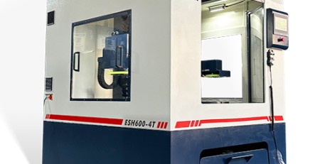
Semiconductor materials are the bedrock of modern electronics, each demanding precise cutting techniques to unleash their full potential. Among these methods, 이다이아몬드 와이어 절단기emerges as a game-changer in semiconductor fabrication.
규소 (Si):
규소, the workhorse of the semiconductor industry, is often cut using diamond wire cutting machines. This method ensures clean cuts with minimal damage, vital for producing integrated circuits and microchips.
For compounds like gallium arsenide, known for its use in high-frequency applications, the diamond wire cutting machine excels. Its precision and low heat generation make it ideal for shaping GaAs components with intricate patterns.
질화 갈륨, valued for its efficiency in power electronics and LEDs, benefits from the diamond wire cutting machine’s capabilities. This technique allows for precise cutting of GaN substrates, essential for high-performance semiconductor devices.
Best Practices for Semiconductor Material Cutting
Precision Equipment:
Invest in high-quality cutting tools and machinery to ensure accurate and clean cuts.
Temperature Control:
Maintain optimal temperature conditions during cutting processes to prevent material damage.
Post-Cutting Inspection:
Conduct thorough inspections post-cutting to guarantee the quality and integrity of the materials.
결론
In the dynamic landscape of semiconductor manufacturing, the cutting of materials stands as a crucial step in the production process. By adopting the best cutting methods and practices, manufacturers can ensure the quality, 정밀, and reliability of semiconductor devices, driving innovation and advancement in the industry.
Through this guide, we aim to shed light on the significance of precision cutting in semiconductor manufacturing and provide insights into the best practices and techniques for achieving optimal results. 기억하다, in the world of semiconductors, every cut counts towards a brighter, more interconnected future.
자주 묻는 질문
What is the best cutting method for semiconductor materials?
For most semiconductor crystals, diamond wire sawing offers the best combination of narrow kerf, low sub-surface damage and throughput; brittle compounds like GaAs especially benefit from its low cutting force.
Why do different semiconductors need different cutting techniques?
They differ in hardness, brittleness and thermal sensitivity — silicon is well understood, while SiC and GaN are far harder, and GaAs is softer but extremely fragile.
Why is precision cutting so important in semiconductor manufacturing?
Surface damage and thickness variation created at slicing carry through lapping, polishing and lithography, directly affecting device yield.
엔솔 엔지니어링 팀이 검토한 기술 내용 — 다이아몬드 와이어 루프 제조업체 10+ 다년간의 생산 경험을 가진 회사.


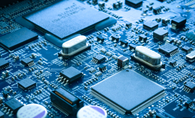
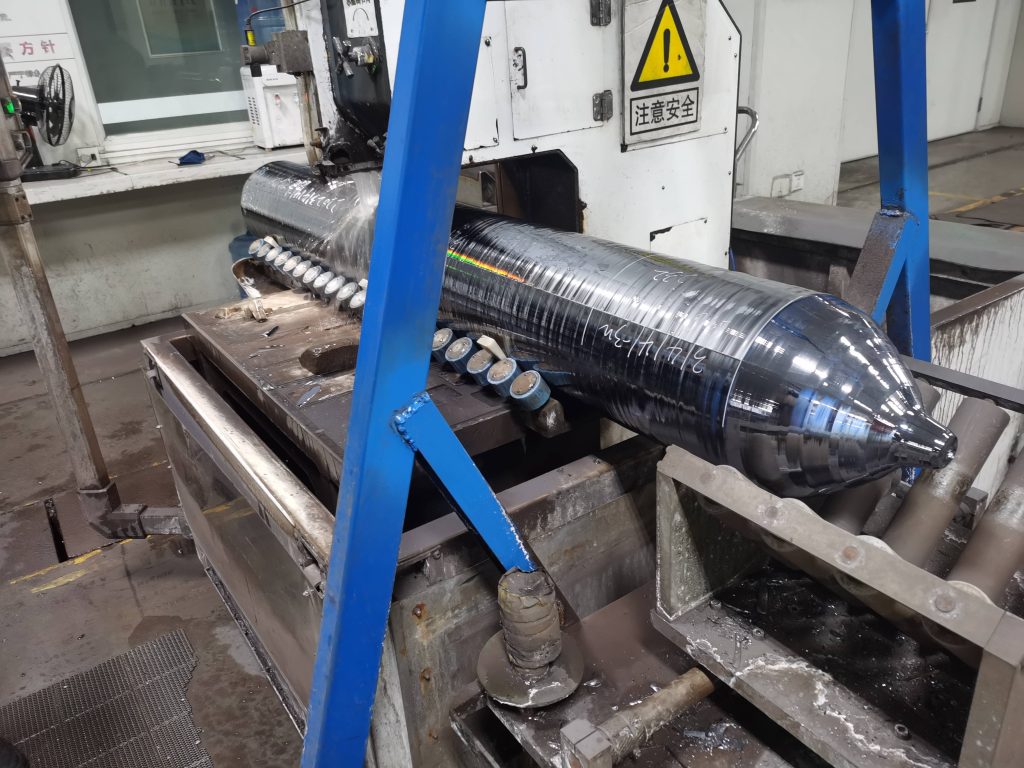


 질화 갈륨, valued for its efficiency in power electronics and LEDs, benefits from the diamond wire cutting machine’s capabilities. This technique allows for precise cutting of GaN substrates, essential for high-performance semiconductor devices.