정밀 제조 분야에서는, 단단한 재료를 얇게 절단하는 것만큼 중요한 공정은 거의 없습니다, 균일한 웨이퍼들. 마이크로칩용 실리콘이든, 전자기기용 세라믹 기판이든, 산업용 응용을 위한 희토류 자석이든, 웨이퍼 톱 공정은 현대 마이크로제조의 핵심입니다.
실리콘 웨이퍼 절단 — 실리콘 웨이퍼 소잉 또는 단순히 웨이퍼 절단 공정이라고도 불리며 — 는 성장한 단결정 잉곳을 칩과 태양전지에 사용되는 얇은 디스크로 만드는 생산 단계입니다. If you are asking how silicon wafers are cut, the short answer is a diamond wire loop running at 10–25 m/s, where wafer thickness and total thickness variation (TTV) are set by wire tension and feed rate. The same physics governs cutting silicon wafers for photovoltaics and for semiconductor substrates; only the thickness target and the tolerance for subsurface damage differ.
But the wafer saw process isn’t a single method. It includes techniques like다이아몬드 와이어 루프 절단, EDM wire cutting, and even compact table top cutter machines for R&D and small-batch production.
주요 요점
A diamond wire loop cuts silicon with a 100–300 µm steel wire electroplated or resin-bonded with diamond grit, running at 10–25 m/s under continuous coolant.
Diamond wire replaced ID blades and slurry sawing mainly because of kerf loss — a narrower cut means more wafers per ingot, which is the dominant cost lever in silicon.
The three defect modes to control are wire breakage and wear, surface micro-cracks, and wire bow caused by uneven tension.
Silicon wafer slicing, silicon wafer sawing and the wafer cutting process all describe the same production step: cutting silicon wafers from a monocrystalline ingot with a diamond wire. Production targets are typically 120–250 µm kerf loss with TTV held under 10 μm의.
– EDM wire cutting as an alternative for conductive materials
– Table top cutter machines for laboratory and prototyping use
자세히 살펴보겠습니다:
1. What is a Wafer?
Before discussing how wafers are cut, we need to understand what a wafer actually is.
A wafer is a thin, flat disc of semiconductor material — most commonly silicon — on which microelectronic devices are built. Wafers serve as the substrate for integrated circuits (IC를), 태양 전지, LEDs, and MEMS (microelectromechanical systems).
Typical Wafer Sizes
Wafers have grown in diameter over decades:
– 1 inch to 2 인치 (early 1960s)
– 4 인치 (100밀리미터), 6 인치 (150밀리미터), 8 인치 (200밀리미터)
– 12 인치 (300밀리미터) – industry standard today
– 18 인치 (450밀리미터) – emerging but rare
Thickness is typically between 500–800 microns, but after polishing and backgrinding, finished IC wafers can be as thin as 50–100 microns.
정밀 절단이 중요한 이유
A single wafer can yield thousands of individual chips (dies). If the cutting process (dicing) is inaccurate, you lose chips, reduce yield, and increase costs. That’s why the wafer saw process must be extremely precise — often within ±1–5 microns.
2. Wafer Saw Process (다이아몬드 와이어 루프)
Now let’s focus on the core of our topic: the wafer saw process using a다이아몬드 와이어 루프.
Traditional vs. Diamond Wire Sawing
Historically, wafers were cut from ingots using inner-diameter (ID) blades — circular saws with diamond-impregnated rims. But ID blades have limitations:
– Wide kerf (material loss)
– Slow cutting speed
– Surface damage
Enter diamond wire sawing.
How Diamond Wire Loop Works
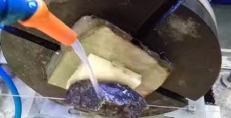
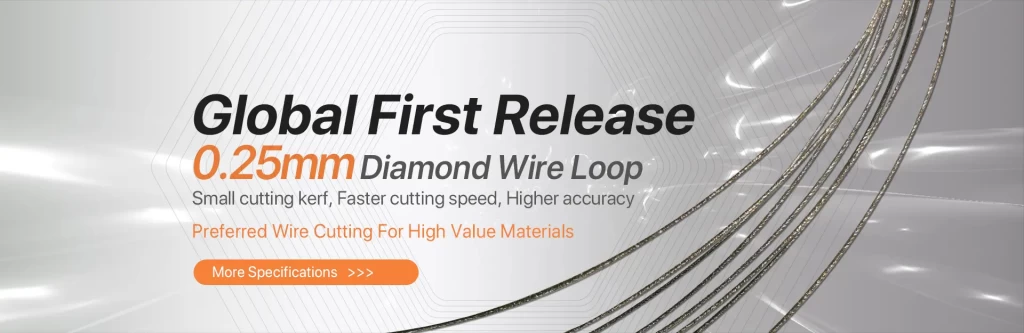
A diamond wire loop consists of a thin steel wire (typically 100–300 microns in diameter) electroplated or resin-bonded with diamond grit. The wire is formed into a continuous loop and driven by pulleys at high speed (10–25 m/s).
As the wire moves, the diamond grit grinds through the material via a three-body abrasion mechanism. 냉각수 (usually deionized water or oil-based fluid) removes debris and heat.
Key Advantages of Diamond Wire Loop for Wafer Sawing
Criterion
다이아몬드 와이어 루프
EDM 와이어 절단
Table Top Cutter (다이아몬드 와이어)
Material type
Non-conductive & hard
Conductive only
Same as diamond wire loop
Typical kerf
120–250 µm
50–150 µm
150–300 µm
표면 마감
좋음 (Ra 0.2–0.5 µm)
우수 (Ra 0.05–0.2 µm)
좋음 (Ra 0.3–0.6 µm)
절삭 속도
Fast (2–10 mm/min)
느리게 (0.5–3 mm/min)
중간 (1–5mm/분)
Equipment cost
높음 (산업용) / 보통 (tabletop)
Medium to High
Low to Medium
최적용
Silicon wafers, 도예, 사파이어
Tool steel, carbide, 타이타늄
R&D, small ingots, fragile materials
Step-by-Step Wafer Saw Process (Ingot to Wafer)
1.Ingot Growth – Single-crystal silicon ingot is grown via Czochralski or Float Zone method.
Grinding – Ingot is ground to precise diameter.
Wire Sawing – Diamond wire loop slices the ingot into individual wafers.
Edge Rounding – Wafer edges are chamfered to prevent chipping.
Lapping – Removes saw marks and flattens the wafer.
Etching – Removes damaged surface layer.
Polishing – Creates mirror-like surface for lithography.
Applications Beyond Silicon
Diamond wire loop sawing isn’t only for실리콘 웨이퍼. It’s also used for:
– 탄화규소 (원문대로) – wide-bandgap semiconductor
– Gallium arsenide (가스(GaAs)) – RF and LED applications
– Sapphire – for LED substrates and watch crystals
– Ceramic substrates – alumina, 지르코니아
– Quartz and glass – optical and MEMS wafers
3. EDM 와이어 절단 (A Complementary Technology)
While diamond wire sawing is excellent for non-conductive and hard materials, EDM wire cutting (방전 가공) offers a completely different mechanism.
What is EDM Wire Cutting?
EDM wire cutting uses a thin, electrically charged brass or copper wire to erode conductive materials through a series of rapid electrical sparks. The wire never touches the workpiece — instead, sparks jump across a small gap, melting and vaporizing tiny particles.
작동 원리
Wire electrode (0.05–3 mm diameter) is continuously fed from a spool.
Deionized water acts as a dielectric fluid, flushing away debris and controlling sparks.
CNC controls move the workpiece relative to the wire.
Sparks occur thousands of times per second, gradually cutting through metal.
When to Use EDM Wire Cutting vs. Diamond Wire Sawing
Material Type
Recommended Method
규소, 질그릇의, 잔, 사파이어
다이아몬드 와이어 루프
Steel, carbide, 타이타늄, Inconel
EDM wire cutting
자성 재료 (NdFeB, 에스엠코)
Both possible; EDM avoids mechanical stress
PCD (polycrystalline diamond)
EDM (diamond is conductive if doped)
Advantages of EDM Wire Cutting
No mechanical contact → no stress or burrs
Cuts extremely hard metals (HRC 60+)
높은 정밀도 (±1–2 microns)
Can cut complex 2D shapes (not just straight slices)
While EDM is rarely used to slice silicon ingots (silicon is only semi-conductive and EDM works poorly on high-resistivity Si), it is used for:
Cutting metalized ceramic substrates
Dicing copper-clad laminates
Slicing tungsten, molybdenum, or Kovar parts used in semiconductor
4. Table Top Cutter Machine
Not every wafer or material cutting job requires a massive industrial saw. For R&D labs, universities, small foundries, and prototype shops, a table top cutter machine is the perfect solution.
Typical Features
Compact footprint (fits on a lab bench)
Adjustable cutting speed and feed rate
Small cutting capacity (typically up to 50–100 mm diameter ingots or blocks)
Integrated coolant system (recirculating or gravity-fed)
Digital readout or CNC control (on high-end models)
Advantages for R&D and Small-Batch Production
Low cost – fraction of industrial wire saws
Flexibility – cut silicon, 도예, 잔, PCB, 자석, 금속
Quick setup – change materials in minutes
Minimal waste – ideal for expensive materials like GaAs or SiC
1. Understanding Monocrystalline Silicon
Before diving into the cutting process, let’s briefly discuss monocrystalline silicon and why it requires specialized cutting techniques.
1.1 What isMonocrystalline Silicon? (You can also click the link to learn more details via Wikipedia.)
Monocrystalline silicon is a highly pure form of silicon with a single, continuous crystal lattice structure. It is produced using the Czochralski (CZ) method or the Float Zone (FZ) 메서드, resulting in cylindrical ingots.
1.2 Why Precision Cutting is Critical
– 반도체 산업: Silicon wafers must have ultra-smooth surfaces(nanometer-level roughness) for microchip fabrication.
-Photovoltaic Industry: Solar cells require thin, 균일한 웨이퍼들(typically 160-180µm) to maximize efficiency.
– 최소한의 절단 손실: Reducing material waste during cutting improves cost efficiency.
Traditional cutting methods like ID saws (inner diameter saws) and multi-wire slurry saws have been replaced by diamond wire saw cutting due to superior performance.
4. 과제 & Solutions in Diamond Wire Saw Cutting
Despite its advantages, 다이아몬드 와이어 톱faces some challenges:
4.1 Wire Breakage & Wear
– Cause: Excessive tension, abrasive wear, or coolant failure.
The wafer saw process is a cornerstone of modern electronics manufacturing. From growing For conductive materials, EDM wire cutting offers a complementary non-contact method capable of slicing hardened steels, carbides, and superalloys with micron-level accuracy.
And for those working in R&D, prototyping, or small-scale production, a table top cutter machine provides an affordable, flexible entry point into high-precision cutting — without the floor space or budget of an industrial wire saw.
Whether you’re manufacturing 300mm silicon wafers for AI processors or cutting a small alumina substrate on a lab bench, understanding the strengths and limitations of diamond wire loop, EDM, and table top cutters will help you select the right tool for the job.a silicon ingot to slicing it into hundreds of thin wafers using a diamond wire loop, every step demands precision, cleanliness, and reliability.
자주 묻는 질문
How are silicon wafers cut from an ingot?
The ingot is grown by the Czochralski or Float Zone method, ground to a precise diameter, then sliced by a diamond wire loop. After sawing, wafer edges are chamfered to prevent chipping, and the wafers are lapped and polished.
What is TTV in wafer cutting?
TTV (total thickness variation) is the difference between the thickest and thinnest points on a wafer. It is the headline metric for wafer sawing quality because downstream lithography needs a flat, uniform surface.
Why did diamond wire replace slurry sawing?
Fixed-diamond wire gives a narrower kerf, a cleaner process with no loose abrasive to manage, 주괴당 더 많은 웨이퍼. Slurry sawing wastes more silicon per cut and carries higher consumable and disposal costs.
What controls breakage when cutting thinner wafers?
Real-time tension monitoring, correctly sized diamond grit, and clean filtered coolant. As wafers drop below 150 μm의, tension stability and feed control matter more than cutting speed.
What is the difference between diamond wire sawing and EDM wire cutting for wafers?
Diamond wire cuts non-conductive and hard materials with a 120–250 µm kerf at 2–10 mm/min and Ra 0.2–0.5 µm. EDM wire cutting only works on conductive materials, is slower at 0.5–3 mm/min, but produces a finer finish of Ra 0.05–0.2 µm.
What wire diameter is used for silicon wafer cutting?
Typically 100–300 µm steel core wire, carrying diamond grit in the 30–100 µm range, applied by electroplating or resin bonding. Thinner wire reduces kerf loss but needs tighter tension control.
How thin can silicon wafers be cut?
Production solar wafers are commonly 160–180 µm, next-generation cells are moving below 150 μm의, and sub-100 µm wafers are the current development target. Each step down demands finer wire and tighter process control.
What causes wire bow, and how is it corrected?
Wire bow is a wavy cut caused by uneven wire tension across the cut. It is corrected with advanced wire guidance systems that apply dynamic tension control throughout the cut.
엔솔 엔지니어링 팀이 검토한 기술 내용 — 다이아몬드 와이어 루프 제조업체 10+ 다년간의 생산 경험을 가진 회사.

 Typical Wafer Sizes
 What is EDM Wire Cutting?
 Monocrystalline silicon is a highly pure form of silicon with a single, continuous crystal lattice structure. It is produced using the Czochralski (CZ) method or the Float Zone (FZ) 메서드, resulting in cylindrical ingots.