태양광 산업용 끝없는 다이아몬드 와이어 루프 & 반도체
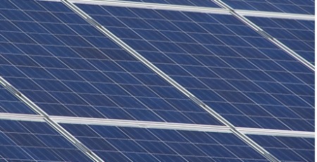
The global transition toward clean energy and advanced computing has placed unprecedented pressure on the supply chains of the photovoltaic (태양광 발전) solar and semiconductor industries. At the heart of both sectors lies a single, foundational material: high-purity silicon. Whether it is monocrystalline silicon grown for high-efficiency solar cells or ultra-pure silicon ingots destined for microchips, these crystals must be sliced into incredibly thin, 기능적 장치로 가공되기 전 완벽한 웨이퍼.
그렇지만, silicon is notoriously brittle and expensive to grow. As solar panels demand thinner wafers to reduce costs and semiconductor nodes shrink to handle higher frequencies, traditional slicing methods are reaching their physical limits.
To overcome these boundaries, leading manufacturers are shifting away from legacy tools and embracing Endless Diamond Wire Loop 기술. This high-speed precision cutting method is rewriting the rules of material yield, 표면 품질, and throughput in wafer manufacturing.
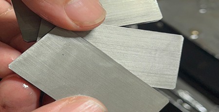
Once the ingot is grown, 실리콘 웨이퍼 절단 decides how much of that expensive crystal ends up as saleable wafers.
The High-Stakes Challenge of Silicon Wafering
Slicing silicon ingots into wafers is one of the most critical and cost-sensitive steps in the entire production line. Because silicon has zero plasticity, forcing a blade or a slow tool through it creates immense localized stress.
When using legacy cutting methods—such as inner-diameter (ID) saws or traditional slurry-based reciprocating wire saws—manufacturers face three major roadblocks:
1. Excessive Material Waste (Kerf Loss)
Silicon ingots require an immense amount of energy and time to grow in crystallization furnaces. Traditional thick blades or loose abrasive slurry wires create a wide cutting path (kerf). This path turns up to 30% 받는 사람 40% of the precious silicon ingot into useless, non-recyclable silicon sawdust (swarf) and slurry. In high-volume PV manufacturing, minimizing this waste is the single fastest way to lower the cost-per-watt of solar modules.
2. 내부 손상 (SSD) and Micro-Cracks
The mechanical shock and heavy feeding force of traditional saws telegraph micro-fractures deep into the interior of the silicon wafer. This sub-surface damage compromises the mechanical strength of the wafer. During subsequent automated handling or chemical etching phases, these micro-cracked wafers easily warp or shatter, severely degrading the factory’s total yield.
3. Strict Geometric Tolerances
Modern photovoltaic cells (especially N-type TOPCon and Heterojunction technologies) and semiconductor devices require wafers with absolute flatness, uniform thickness, and near-zero Total Thickness Variation (TTV). Reciprocating saws that constantly decelerate and reverse direction suffer from wire vibration, which leaves waves and saw marks across the wafer surface, requiring extensive secondary polishing.
The Solution: Endless Diamond Wire Loop Technology
To solve these compounding issues, the photovoltaic and semiconductor sectors are integrating Endless Diamond Wire Loops.
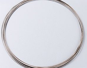
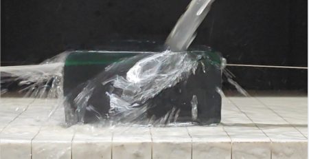
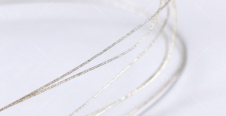
An endless diamond wire loop consists of a high-strength, flexible steel wire core that is welded into a continuous, seamless ring. Its outer surface is permanently electroplated with precisely graded microscopic industrial diamond particles. Instead of moving back and forth in a reciprocating motion, the loop runs continuously in a single, uninterrupted direction over a specialized high-speed pulley system.
This unidirectional, high-speed configuration delivers a massive technological leap forward due to three distinct physical advantages:
Ultra-High Linear Speeds and Gentle Micro-Grinding
While traditional open-loop wire saws travel at relatively low speeds, an endless diamond wire loop can rotate at staggering linear velocities—often between $30\text{ 엠/초}$ and $60\text{ 엠/초}$.
This immense speed completely alters the mechanics of the cut. Because the wire moves so fast, the contact time between any single diamond crystal and the silicon matrix is incredibly brief, dropping the feeding pressure to near zero. The process transitions from a brutal mechanical “톱질” force into a gentle, continuous micro-grinding action. This eliminates the mechanical shock factors that cause micro-fractures, allowing for sharp, chip-free wafer edges.
Ultra-Thin Wires for Maximum Wafer Yield
Because the endless loop maintains perfect, steady tension without the violent “vibration jerk
” associated with reversing directions, the core steel wire can be made exceptionally thin. Today’s industrial loops feature wire diameters down to $0.20\text{ 밀리미터}$ or less.
The Strategic Benefit: A narrower cutting wire means a narrower kerf. By reducing material waste on every single slice, manufacturers can extract significantly more usable wafers out of a single silicon ingot, maximizing raw material utilization and instantly driving down production costs.
Pristine Surface Quality and Minimal Post-Processing
The continuous, smooth motion of a closed-loop system entirely eliminates the prominent “saw marks” and deep surface gouges typical of slower cutting methods. The resulting surface roughness ($R_a$) and Total Thickness Variation (TTV) are remarkably low.
For the photovoltaic sector, this clean “as-cut” surface means wafers can go directly into texturing and doping phases. For the semiconductor sector, it slashes the time and labor required for downstream Chemical Mechanical Planarization (CMP) and fine polishing stages.
태양광 발전 & Semiconductor Wafer Slicing Comparison
| Performance Parameter | Traditional Slurry / ID Saws | Endless Diamond Wire Loop |
| Cutting Action | Low-speed mechanical shearing | High-speed, low-force micro-grinding |
| Wire/Blade Thickness | Thick ($0.5\텍스트{ 밀리미터}$ – $1.2\텍스트{ 밀리미터}$) | Ultra-thin ($0.18\텍스트{ 밀리미터}$ – $0.30\텍스트{ 밀리미터}$) |
| Material Yield (Kerf Loss) | 미흡 (High volume of silicon waste) | 우수 (Maximum wafers per ingot) |
| 표면 마감 (TTV / $R_a$) | High variation, prominent saw marks | Extremely flat, near pre-polished surface |
| 내부 손상 (SSD) | Deep micro-cracking risk | Negligible, preserving wafer structural integrity |
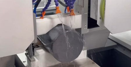
For a full parameter walk-through of diamond wire loop slicing of silicon rods (φ330 mm, 10 mm slices), see our engineering case study.
- Photovoltaic and semiconductor wafering share one bottleneck: slicing hard, brittle silicon with minimal kerf loss and sub-surface damage.
- Endless diamond wire loops cut at ultra-high linear speeds with a gentle micro-grinding action that limits micro-cracks and sub-surface damage.
- Ultra-thin diamond wires maximize wafer yield per ingot — the single biggest cost lever in both the PV and semiconductor industries.
결론: Driving Next-Generation Clean Energy and Computing
As the green energy transition accelerates and semiconductor nodes shrink further, manufacturing efficiency must evolve. Wasting premium, 에너지 집약적인 결정질 실리콘은 경쟁이 치열한 글로벌 시장에서 더 이상 받아들여지지 않는다.
끝없는 다이아몬드 와이어 루프는 태양광 및 반도체 분야에서 실리콘 절단의 결정적 기술로 입증되었다. 재료 취성을 극복하며, 원자재 수율 최적화, 완벽한 표면 형상을 제공함, 이 첨단 절단 기술은 전 세계 청정 태양 에너지와 고성능 컴퓨팅의 미래를 지지하는 중요한 기둥.
자주 묻는 질문
끝없는 다이아몬드 와이어 루프란 무엇인가?
다이아몬드 연마재로 코팅된 고장력 강철 와이어의 닫힌 루프, 단단하게 절단하기 위해 고속으로 연속 작동, 실리콘과 같은 취성 재료, SiC와 사파이어.
왜 웨이퍼 가공에서 절단 손실이 그렇게 중요한가?
절단 하나당 먼지가 된 실리콘. Thinner wire and a narrower cut mean more wafers per ingot, 이는 각 웨이퍼의 비용을 직접 낮춘다.
서브서피스 손상이란 무엇인가 (SSD)?
SSD는 절단된 표면 아래에 남아 있는 미세 균열층으로, 연마나 에칭으로 제거해야 한다. 다이아몬드 와이어의 부드러운 미세 연삭은 이 층을 얕게 유지한다, 후속 공정 시간을 절약한다.
하나의 와이어 루프 플랫폼이 PV와 반도체 웨이퍼 절단 모두에 사용할 수 있는가?
예. 절단 원리는 동일하다; 와이어 직경, 속도, 텐션과 냉각수는 각 산업의 웨이퍼 크기와 두께 사양에 맞춰 조정된다.
엔솔 엔지니어링 팀이 검토한 기술 내용 — 다이아몬드 와이어 루프 제조업체 10+ 다년간의 생산 경험을 가진 회사.