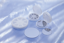
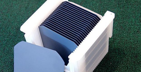
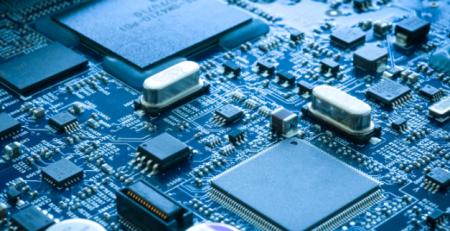
A semiconductor chip, Обычно называется интегральной схемой, представляет собой полупроводниковое устройство, изготовленное на полупроводниковой пластине с помощью таких процессов, как травление, проводка, и создание шаблонов для достижения определенных функций. Больше, чем кремниевые чипы, К распространенным полупроводниковым материалам относится арсенид галлия, нитрид галлия, и карбид кремния.
Последний обзор: Сентябрь 2026
Основные выводы
Semiconductors are materials with conductivity between conductors and insulators, forming the basis of all integrated circuits.
Beyond silicon, key semiconductor types include gallium arsenide (GaAs), нитрид галлия (Гань) и карбид кремния (Так), each with distinct application niches.
GaAs serves RF and optoelectronics, GaN serves high-frequency power, and SiC serves high-voltage, high-temperature power devices.
Процесс производства полупроводников сродни превращению базовых материалов в золото, в основном включает в себя серию обработок на кремниевых пластинах. По сути, через эпитаксиальный рост, фотолитография, офорт, допинг, и полировка, the required circuits are formed on the silicon wafer, transforming it into a chip.
Types of Semiconductors
Semiconductor materials are electronic materials used in the production of semiconductor devices and integrated circuits, forming the foundation of the semiconductor industry.
With the emergence of new semiconductor materials, advancements in power electronics technology, and improvements in manufacturing processes, semiconductors have undergone three generations of changes. Gallium arsenide (GaAs) and gallium nitride (Гань), as well as silicon carbide (Так) Полупроводников, represent the second and third generations of semiconductors, соответственно.
Compared to the first-generation semiconductor silicon (Си), these materials exhibit superior performance in aspects such as high frequency and high temperature.
Compound semiconductor chips, known for their excellent high-frequency performance, are commonly used in the production of power semiconductors, with their applications becoming increasingly widespread. Through techniques such as frequency conversion, voltage transformation, current modulation, power amplification, and management, these chips serve two primary functions: amplification and switching.
Настоящее время, over 75% of electrical energy applications require power conversion before being supplied to devices. Their applications continue to expand.
Amplification involves converting low-frequency power into high-frequency power, leveraging amplification to drive motors with low power efficiently. Switching entails toggling circuits on and off, with faster switching speeds enabling precise control.
Amplification: Converting low-frequency power into high-frequency power, making full use of amplification allows for driving motors with low power effectively.
Switching:Toggling the circuit on and off, the faster the switching speed, the more precise control can be achieved.
Gallium Arsenide Semiconductor
Gallium arsenide semiconductor chips are primarily used in microwave power devices, which operate in the microwave frequency range (between 300 и 300,000 megahertz). Due to the inherent physical limitations of silicon (Си), it can only be applied at frequencies below 1 GHz. Однако, в последние годы, the rapid development of wireless high-frequency communication products has propelled gallium arsenide to the forefront, showcasing characteristics such as high operating frequencies, electron mobility rates, resistance to natural radiation, and low power consumption, making it widely used in the field of microwave communication.
Given the high-frequency transmission characteristics of gallium arsenide, it has seen rapid growth not only in mobile phone applications but also in WiFi modules embedded in laptops, tablets, fixed network wireless transmission, as well as fiber optic communication, satellite communication, point-to-point microwave communication, cable television, automotive navigation systems, and collision avoidance systems. These applications often employ varying numbers of power amplifiers (ranging from 1 Кому 4 chips), driving the significant advancement of gallium arsenide.
Gallium Nitride Semiconductor
Gallium nitride material, with a bandgap width of 3.4 eV, is considered a third-generation semiconductor material along with materials like SiC and diamond, known as wide-bandgap semiconductors. Due to its advantages such as a wide bandgap, high breakdown field, large saturation electron velocity, высокая теплопроводность, низкая диэлектрическая проницаемость, Химическая стабильность, and strong radiation resistance, gallium nitride has become one of the preferred materials for high-temperature, high-frequency, и мощные СВЧ-устройства.
Comparison of Gallium Nitride (Гань) with Gallium Arsenide (GaAs) and Silicon (Си):
The increasing demand for high-speed, high-temperature, and high-power semiconductor devices has led to the gradual adoption of gallium nitride material in the semiconductor market. Its primary application areas include:
Renewable Energy Sector:
In the field of renewable energy, gallium nitride plays an extremely important role in integrating wind and solar power into the grid and reducing transmission losses. Green energy, электромобилей, green electronic lighting, and other emerging areas are becoming new hotspots for power device market applications, with strong demand.
Information Communication Equipment Sector:
Enhanced gallium nitride transistors exhibit high radiation resistance, making them suitable for power and communication systems in communication and scientific satellites. Point-to-point communication, satellite communication, various radars, and new industrial/defense applications will benefit from the application of these high-power gallium nitride devices.
4C Industries:
Major domestic IT products are expected to maintain strong market demand, with traditional products like laptops, monitors, printers, televisions, home theater systems, and Blu-ray players, as well as emerging automotive electronics, projected to experience steady growth in the future. As production capacity for electronic products such as air conditioners and energy-efficient motors shifts to the Chinese mainland, the demand for power semiconductors is expected to double.
Smart Grid Sector:
Power semiconductors play a crucial role in improving the overall energy efficiency of the entire power supply chain—from generation, transmission, and distribution to end-user consumption—in the field of smart grids.
Silicon Carbide Semiconductor
Карбид кремния (Так) has become one of the most prominent semiconductor materials due to its outstanding performance under high temperature, высокое давление, and high frequency conditions. It is widely used in power conversion devices such as AC-DC converters and is expected to gradually replace silicon comprehensively in the field of semiconductor power devices, heralding the dawn of the Silicon Carbide Semiconductor era.
Compared to silicon devices, SiC semiconductor chips can reduce power losses by nearly 50%, effectively enhancing power conversion efficiency. SiC devices, with their high conversion efficiency and low heat generation, can reduce the size of cooling systems, leading to overall downsizing of power conversion devices. This is of significant importance for systems like new energy vehicles that require numerous power conversion devices. Следовательно, for systems requiring high conversion efficiency and power density, SiC devices offer unparalleled advantages and are the preferred choice.
Due to its exceptional performance, silicon carbide is particularly suitable for applications requiring high-power conversion, such as deep well drilling, solar inverters (for DC to AC conversion), wind energy inverters, electric and hybrid vehicles, industrial drives, and light rail traction systems.
Fabrication Method:
The semiconductor manufacturing process is akin to turning lead into gold, в основном включает в себя серию обработок на кремниевых пластинах. While a detailed explanation can be quite complex, in simple terms, it involves epitaxial growth, фотолитография, офорт, допинг, and polishing to create the required circuits on the silicon wafer, transforming it into a chip. Steps like photolithography and etching still rely on foreign technologies and the use of foreign patents
Semiconductor processing methods
Four Cutting Technologies: A Comparative Overview:
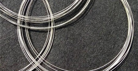
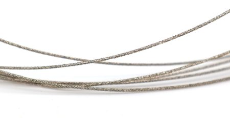
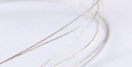
1. Резка петли из алмазной проволоки
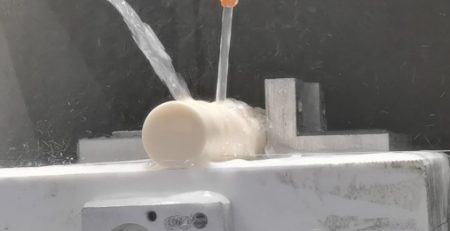
Principle: A fast-moving loop of wire, coated with diamond particles, acts as a cutting tool, grinding through the material. Coolant is often used.
Key Advantage:Low stress, Высокая точность, minimal material waste. Тем “flexible” wire is gentle on brittle materials, enabling clean cuts with almost no edge chipping. It is the preferred method for slicing high-value, твердый, brittle materials like SiC, Гань, сапфир, и оптическое стеклоinto thin wafers.
Limitation:Limited cutting speed. As a grinding process, its material removal rate is slower than thermal methods like laser cutting, making it less efficient for high-volume or rough cutting jobs.
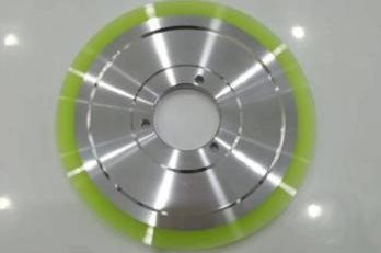
2. Diamond Saw Blade Cutting
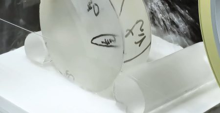
Principle:A rotating circular blade with a diamond-coated edge cuts through the material, similar to a precision stone cutter.
Key Advantage:Proven technology, Высокая эффективность, relatively low cost. It’s the standard method for rough cutting and sizing blocks of silicon and ceramic.
Limitation:High mechanical impact. It can easily cause edge chipping and internal stress or micro-cracks, making it unsuitable for finishing ultra-thin, ultra-hard, or high-value materials.
3. Лазерная резка
Principle:A focused, high-energy laser beam melts, vaporizes, or alters the material, with a gas jet removing the debris.
Key Advantage:Non-contact, no tool wear, very fast, highly flexible. It easily handles complex 2D shapes and can perform “stealth dicing” (separation via internal modification), making it ideal for wafer dicing and shaping silicon, сапфир, и стекла.
Limitation:Creates a heat-affected zone that may change material properties at the cut edge. It can struggle with highly reflective (например., pure copper) or transparent materials. Equipment is expensive.
Principle:Controlled spark discharges between a thin wire electrode and the workpiece generate intense heat, locally melting and vaporizing the material.
Key Advantage:Cuts any conductive material regardless of hardness (например., hardened steel, Карбид вольфрама, conductive ceramics). It achieves very high precision and can create complex shapes.
Limitation:Only works on conductive materials. The process is slow, and it leaves a recast layer on the cut surface.
Summary & Selection Guide
There is no single “best” technology—each is most suitable for specific tasks:
For ultimate cut quality and minimal loss when slicing hard, brittle wafers (например., Так): ChooseПетля из алмазной проволоки Режущий.
For efficient, low-cost rough cutting of hard, brittle blocks: Choose Diamond Saw Blade Cutting.
For high-speed cutting of complex 2D shapes in various materials (including non-metals): Choose Laser Cutting.
For machining intricate shapes in very hard, conductive materials (например., molds): Electrical Discharge Cutting is the only choice.
Current Situation:
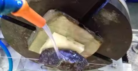
Настоящее время, many technologies require a fresher perspective to be infused, as each step in the process could potentially lead to significant advancements. Regarding one specific aspect, we conducted a experiment on cutting 12-inch ingots two weeks ago. We utilizedЭнсолтулсLimited’sалмазная проволочная пила Технологии, where the wire marks are nearly invisible, and the flatness can be controlled within 3 микрометров. This method addresses many issues related to cutting semiconductor concave surfaces, greatly reducing the difficulty of subsequent polishing and material consumption.
A semiconductor is a material whose electrical conductivity sits between a conductor and an insulator and can be controlled by doping, making it the foundation of integrated circuits.
What are the main types of semiconductor materials?
Silicon dominates general ICs; compound semiconductors include gallium arsenide (RF, optoelectronics), нитрид галлия (high-frequency power) и карбид кремния (высоковольтный, high-temperature power).
Where are SiC and GaN semiconductors used?
SiC is used in EV inverters and high-voltage power modules, while GaN is used in fast chargers, RF power amplifiers and 5G infrastructure.
Основные выводы
Алмазная петлевая проволочная резка обеспечивает высокую точность и тонкую обработку, важна для производства высокоточных оптических компонентов, таких как линзы,... читать далее
Ключевые выводы
Стальные направляющие колесики обеспечивают максимальную жесткость и стабильность размеров для высокоточной резки алмазной проволокой, но передают больше вибрации на... читать далее
Основные выводы
Алмазная проволочная пила режет материалы с помощью высокоскоростной вращающейся проволочной пилы, обеспечивая высокую точность и высокую эффективность по сравнению с.... читать далее
Основные выводы
Производителям фотоэлементов нужно больше пластин на слиток при все более низкой стоимости — именно это обеспечивает резка алмазной проволочной петлей.
Узкий... читать далее
Петли из алмазной проволоки изготавливаются с использованием передовых производственных процессов, в которых алмазы встраиваются в проволочную петлю. Этот... читать далее
Основные выводы
Точная резка имеет первостепенное значение в производстве полупроводников, поскольку повреждения при нарезке распространяются на все последующие процессы.
Разные полупроводниковые материалы требуют разных... читать далее
Основные выводы
Лазерная резка бесконтактная и быстрая, но ее зона, подверженная воздействию тепла, может создавать микротрещины, которые снижают эффективность солнечного элемента.
Алмазная проволока... читать далее