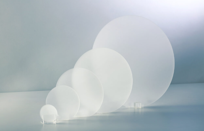
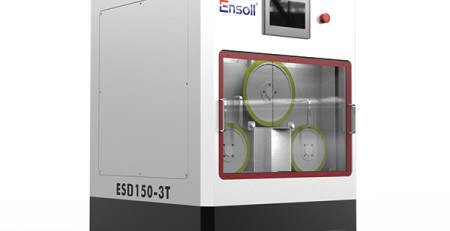
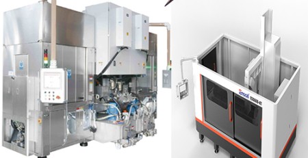
Сапфировые подложки являются критическими компонентами при производстве светодиодов, оптических устройств, и полупроводниковых приложений. Однако, cutting sapphire—a material with a Mohs hardness of 9—poses significant challenges. Traditional methods like blade sawing or laser cutting often lead to cracks, high material loss, and uneven surfaces.
Основные выводы
Сапфир (по шкале Мооса 9) is both extremely hard and brittle: blade sawing and laser cutting often cause cracks, uneven surfaces, and up to 30% Потери материала.
A diamond wire loop can be as thin as 0.1 mm versus a 0.3 mm or wider blade kerf, so more wafers are recovered from every crystal ingot.
The low-force wire cut generates far less mechanical stress, preventing subsurface micro-cracks and leaving a smoother surface that needs less polishing.
Modern machines cut sapphire at 0.5-2 мм/мин, and multi-wire systems can slice hundreds of wafers simultaneously.
Main beneficiaries: LED sapphire substrates, ultra-thin semiconductor wafers (down to about 100 микрометры), and optical windows and lenses.
Петля из алмазной проволокиcutting has emerged as the superior solution, offering higher precision, minimal kerf loss, and reduced subsurface damage. В этой статье, we explore how this advanced technology improves efficiency in sapphire substrate production.
Challenges in Sapphire Substrate Cutting
Before discussing diamond wire loops, it’s essential to understand the difficulties in processing sapphire:
Extreme Hardness – Sapphire is one of the hardest materials, making mechanical cutting difficult.
Brittleness – Improper cutting can cause micro-cracks, reducing substrate quality.
High Precision Requirements – LED and semiconductor industries demand ultra-thin wafers (as low as 100µm) with near-perfect surfaces.
Material Waste – Conventional methods lose up to 30% of the material, increasing costs.
Traditional methods like ID saws (Пилы с внутренним диаметром) and laser cutting struggle with these challenges, leading to higher rejection rates and production inefficiencies.
How Diamond Wire Loop Cutting Works
Diamond wire loop technology uses a thin, flexible wire embedded with diamond particles to slice through sapphire with minimal force. Here’s how it enhances efficiency:
1.Precision Cutting with Minimal Kerf Loss
– The wire diameter can be as thin as 0.1mm, significantly reducing material waste compared to blade saws (which have a kerf of 0.3mm or more).
– This allows more wafers per crystal ingot, lowering production costs.
✅ LED Manufacturing – Producing high-quality sapphire substrates for brighter, more efficient LEDs.
✅ Semiconductor Wafers – Enabling ultra-thin wafers for advanced electronics.
✅ Optical Components – Cutting sapphire windows and lenses with superior surface integrity.
Заключение
Diamond wire loop cutting has revolutionized sapphire substrate processing by improving precision, reducing waste, and increasing production efficiency. As demand for high-performance LEDs and semiconductors grows, this technology will remain a critical tool for manufacturers seeking cost-effective, high-quality solutions.
Interested in optimizing yoursapphire cutting процесс? Contact us today to learn how diamond wire loops can enhance your production line!
Часто задаваемые вопросы
Why is sapphire so difficult to cut?
Sapphire rates 9 on the Mohs hardness scale and is highly brittle, so conventional blade or laser cutting easily produces micro-cracks and high rejection rates. The LED and semiconductor industries also demand ultra-thin wafers with near-perfect surfaces, which leaves almost no margin for error.
How does a diamond wire loop reduce sapphire material waste?
Проволока может быть такой же тонкой, как 0.1 миллиметр, по сравнению с шириной реза лезвием 0.3 мм или более. Традиционные методы теряют до 30% ингота, в то время как узкий рез проволоки превращает больше кристалла в используемые пластины и снижает производственные затраты.
Повреждает ли резка сапфира алмазной проволокой поверхность??
Нет. Поскольку проволока режет с очень малой силой, она создает меньше механического напряжения, чем абразивные пилы, что предотвращает образование микротрещин под поверхностью. Полученная поверхность более гладкая и требует меньше полировки в дальнейшем.
Какие отрасли используют подложки из сапфира, разрезанного алмазной проволокой??
Производство светодиодов использует их для более ярких, и более эффективных чипов; полупроводниковая промышленность использует ультратонкие сапфировые пластины для передовой электроники; а производители оптики режут сапфировые окна и линзы с превосходной целостностью поверхности.
ключевые выводы
При приготовлении полупроводниковых пластин, однокристаллические кремниевые слитки перерабатываются в голые пластины с высокой точностью поверхности для литографии.
слиток... читать далее
Основные выводы
Промышленный сапфир — это корунд (Al2O3) — природный или синтетический — который не достигает качества декоративного драгоценного камня и является... читать далее
Традиционный процесс производства солнечных батарей
Ключевые выводы
Традиционное производство солнечных батарей начинается с изготовления кремниевых пластин и продолжается текстурированием, диффузия, офорт,... читать далее
Ключевые выводы
Одноручная алмазная проволочная пила несёт одну алмазную проволоку на одной руке: flexible for small batches and multi-specification work,... читать далее
Основные выводы
Размеры фотогальванических кремниевых пластин развивались от форматов кремниевых полупроводниковых пластин, при этом PV исторически отставал от полупроводников по стандартам размеров.
Размеры пластин продолжают... читать далее
Основные выводы
Кварцевое стекло — это однокомпонентное кремнеземное стекло, называемое Королем стекла; кварцевое стекло высокой чистоты хорошо пропускает .... читать далее
Введение
В современном производстве, Важность технологий прецизионной обработки становится все более очевидной, особенно в области магнитных материалов.. читать далее