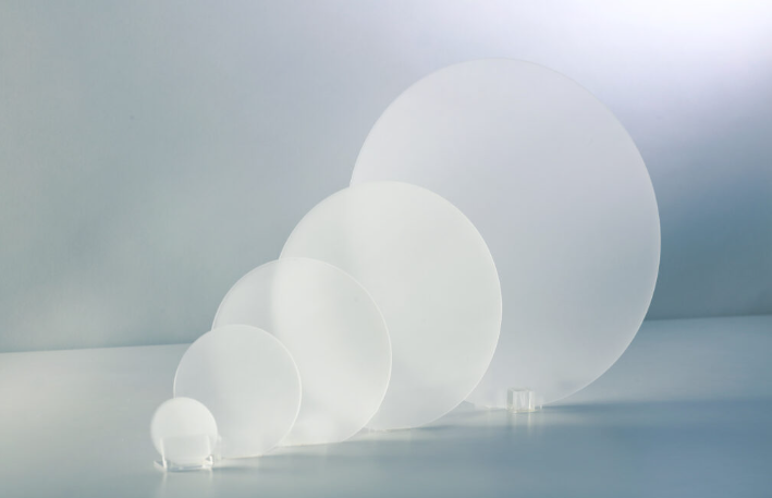
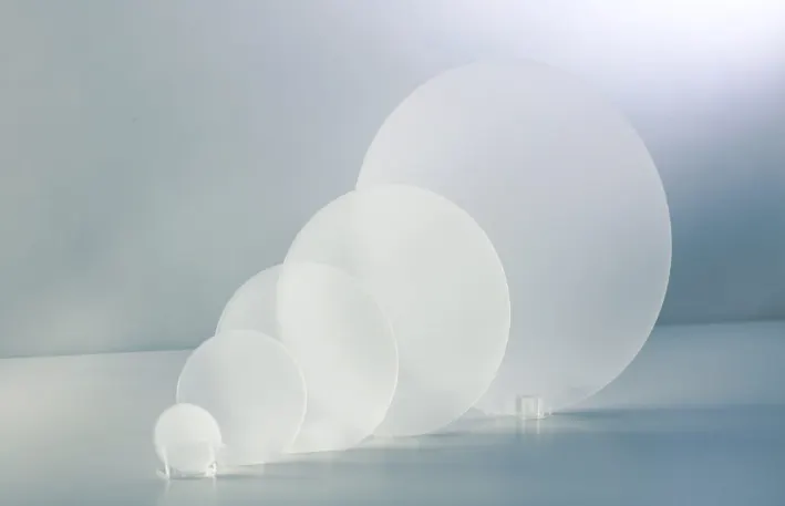
蓝宝石基板是LED制造中关键组件, 光学器件, 以及半导体应用. 然而, cutting sapphire—a material with a Mohs hardness of 9—poses significant challenges. Traditional methods like blade sawing or laser cutting often lead to cracks, high material loss, and uneven surfaces.
关键要点
蓝宝石 (莫氏硬度 9) is both extremely hard and brittle: blade sawing and laser cutting often cause cracks, uneven surfaces, and up to 30% material loss.
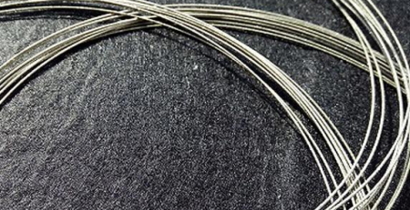
A diamond wire loop can be as thin as 0.1 mm versus a 0.3 mm or wider blade kerf, so more wafers are recovered from every crystal ingot.
The low-force wire cut generates far less mechanical stress, preventing subsurface micro-cracks and leaving a smoother surface that needs less polishing.
Modern machines cut sapphire at 0.5-2 毫米/分钟, and multi-wire systems can slice hundreds of wafers simultaneously.
Main beneficiaries: LED sapphire substrates, ultra-thin semiconductor wafers (down to about 100 微米级), and optical windows and lenses.
金刚石线环cutting has emerged as the superior solution, offering higher precision, minimal kerf loss, and reduced subsurface damage. 本文内容, 我们探讨了这项先进技术如何提高蓝宝石衬底生产的效率.
蓝宝石衬底切割的挑战
在讨论金刚石线圈之前, 了解蓝宝石加工的困难是必要的:
极高硬度 – 蓝宝石是最硬的材料之一, 使机械切割变得困难.
脆性 – 不当切割可能导致微裂纹, 降低衬底质量.
高精度要求 – LED和半导体行业要求超薄晶片 (薄至100微米) 并且表面近乎完美.
材料浪费 – 传统方法会损失多达 30% 材料, 增加成本.
传统方法如内径锯 (内径锯) 和激光切割难以应对这些挑战, 导致更高的废品率和生产效率低下.
金刚线环切割的工作原理
Diamond wire loop technology uses a thin, flexible wire embedded with diamond particles to slice through sapphire with minimal force. Here’s how it enhances efficiency:
1.Precision Cutting with Minimal Kerf Loss
– The wire diameter can be as thin as 0.1mm, significantly reducing material waste compared to blade saws (which have a kerf of 0.3mm or more).
– This allows more wafers per crystal ingot, lowering production costs.
✅ LED Manufacturing – Producing high-quality sapphire substrates for brighter, more efficient LEDs.
✅ Semiconductor Wafers – Enabling ultra-thin wafers for advanced electronics.
✅ Optical Components – Cutting sapphire windows and lenses with superior surface integrity.
结论
Diamond wire loop cutting has revolutionized sapphire substrate processing by improving precision, reducing waste, and increasing production efficiency. As demand for high-performance LEDs and semiconductors grows, this technology will remain a critical tool for manufacturers seeking cost-effective, high-quality solutions.
Interested in optimizing yoursapphire cutting 工艺? Contact us today to learn how diamond wire loops can enhance your production line!
常见问题
Why is sapphire so difficult to cut?
Sapphire rates 9 on the Mohs hardness scale and is highly brittle, so conventional blade or laser cutting easily produces micro-cracks and high rejection rates. The LED and semiconductor industries also demand ultra-thin wafers with near-perfect surfaces, which leaves almost no margin for error.
How does a diamond wire loop reduce sapphire material waste?
The wire can be as thin as 0.1 毫米, compared with a blade kerf of 0.3 mm or more. Conventional methods lose up to 30% of the ingot, while the narrow wire kerf converts more of each crystal into usable wafers and lowers production cost.
Does diamond wire loop cutting damage the sapphire surface?
不. Because the wire cuts with very low force, it generates less mechanical stress than abrasive saws, which prevents subsurface micro-cracks. The resulting surface is smoother and requires less polishing afterward.
Which industries use diamond-wire-cut sapphire substrates?
LED manufacturing uses them for brighter, more efficient chips; the semiconductor industry uses ultra-thin sapphire wafers for advanced electronics; and optics producers cut sapphire windows and lenses with superior surface integrity.