碳化硅切割: 金刚石线锯指南
在先进半导体的高要求领域, 性能和效率至关重要, 有一种材料成为关键推动因素: 碳化硅 (原文如此). Known for its exceptional hardness (仅次于金刚石), 高导热性, and superior electrical properties, SiC is the cornerstone of next-generation power electronics. 然而, its very advantages make it notoriously difficult to process. This is where the transformative power of the 金刚石绳锯 comes into play, acting as the scalpel that unlocks the potential of this super material.
- Silicon carbide ranks about 9.2–9.5 on the Mohs scale — close to diamond — and combines that hardness with brittleness, so blade and laser cutting both leave damage.
- Diamond wire is the matching tool: it cuts SiC cold with a continuous abrasive action instead of impact or heat, which avoids the micro-cracking that ruins SiC wafers.
- Blade dicing typically leaves more than 20 µm of edge chipping on SiC. Diamond wire holds chipping to near zero, and that difference is what protects yield on power devices and RF chips.
- In production, switching from laser to diamond wire on SiC MOSFET cutting lifted yield from 78% 自 93% at 500 mm/min — the gain came almost entirely from eliminating crack-induced failures.
- Wire can run as fine as 0.2 毫米. Because SiC boules are expensive, that narrow kerf converts directly into more wafers per crystal.
- For SiC/GaN work, specify wire 0.1–0.3 mm in diameter with 10–20 µm diamond grit, and hold machine vibration below 0.1 µm — grit cuts the material, but vibration is what creates the micro-cracks.
- GaN fails differently from SiC: it is less hard but has high fracture toughness, so it cracks rather than abrades. Low-vibration wire cutting matters more on GaN than raw abrasive hardness.
The SiC Challenge: 一种难以驯服的材料
在碳化硅(SiC)成为高效电动车逆变器或紧凑型电网变流器的核心之前, 它必须被从实心晶棒中精确切片成薄晶片. 传统切割方法, 例如,使用磨料浆料锯, 切割SiC时非常困难. 它们速度慢, 产生大量废料, 和, 最关键的是, 会在脆性晶体中引发亚表面微裂纹和高应力. 这些缺陷会损害性能, 降低最终芯片的良率和可靠性. 业内需要一种能与SiC硬度匹配、且同样精确温和的解决方案.
 为什么金刚石线锯是SiC的完美匹配
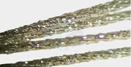
金刚石线锯的工作原理既简单优雅,又极其有效: 一条连续循环的钢丝, 电镀有金刚石颗粒, moves at high speed to perform a clean, linear cut. For SiC, this technology offers a suite of unbeatable advantages:
- Minimized Kerf Loss, Maximized Yield: The diamond wire can be incredibly thin (as fine as 0.2mm). This creates an extremely narrow cut path, or “kerf.” Given the high cost of SiC boules, every millimeter saved translates directly into more wafers per crystal and substantial material cost savings. This efficiency is fundamental for making SiC technology more commercially viable.
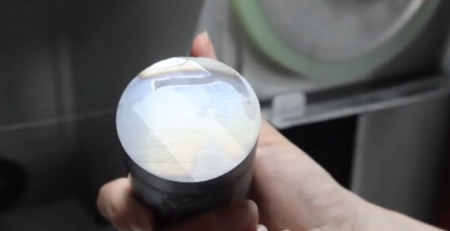
- 优越的表面完整性: 闭环系统的连续, controlled cutting action of the wire generates minimal mechanical and thermal stress. The result is a wafer surface with exceptional as-cut quality—smoother and with dramatically fewer micro-cracks compared to traditional methods. This “low-damage” surface means the subsequent, time-consuming grinding and polishing steps can be significantly reduced, accelerating the entire production workflow.
- Uncompromised Crystal Quality: Perhaps the most critical advantage for semiconductor applications is the preservation of SiC’s intrinsic electrical properties. The clean, low-stress cut ensures the crystalline lattice at the wafer’s edge and surface remains intact. This directly contributes to higher chip performance, better breakdown voltage characteristics, and ultimately, more reliable and powerful electronic devices.
- Cool and Controlled Processing: The cut is typically performed with a water-based coolant, preventing localized overheating that could alter the material’s properties. This “cold cutting” process is essential for maintaining the precise stoichiometry and quality required for high-end semiconductors.
From Wafer to Wonder: The Journey of a Cut SiC Wafer
Once sliced and polished, these pristine SiC wafers become the foundation for a technological revolution. Their primary destination is the fabrication of power semiconductor devices
- Electric Vehicles (电动汽车): SiC MOSFETs and diodes form the core of the main traction inverter. They switch electricity with far less loss than traditional silicon chips, enabling longer driving range, faster charging, and more compact, efficient powertrains.
- 可再生能源: In solar inverters and wind turbine converters, SiC devices handle high voltages and frequencies with exceptional efficiency, minimizing energy loss as green power is fed into the grid.
- 5G & RF Infrastructure: The high-frequency capabilities of SiC make it ideal for radio frequency power amplifiers in the next generation of communication base stations, 实现更快的数据传输.
- 工业电机驱动: 基于SiC的驱动允许更小型化、, 更高效的工业电机控制系统, 从而在制造和自动化中实现显著的节能.
了解金刚石绳锯的硬度和特性
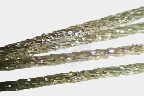
- 金刚石绳锯的硬度归因于嵌入线材中的金刚石颗粒. 钻石以其非凡的硬度而闻名, 被评为最坚硬的天然材料. 当并入绳锯时, 金刚石提供卓越的切削刃,可以毫不费力地穿透和研磨各种材料.

了解碳化硅的硬度和特性
切割碳化硅的挑战
1. 极高的硬度和脆性:
莫氏硬度约为 9.5, 仅次于金刚石和氮化硼, SiC是一种极硬且脆的材料. 传统切削工具磨损快, 导致成本效益低下. 更关键的是, 其脆性使其在机械切割过程中极易产生微裂纹、, 边缘崩裂, 和次表面损伤. 这种损伤层会严重降低最终半导体器件的性能和可靠性.
最后审核: 九月 2026
2. 低切割效率和高工具磨损:
使用金刚石工具 (如金刚石线或金刚石刀片) 几乎是必需的. 然而, even diamond abrasives experience substantial wear when cutting SiC, leading to decreasing cutting rates over time, increased heat generation, and higher consumable costs. The process often requires multiple steps (roughing and finishing) to achieve the desired surface integrity, further reducing overall throughput.
3. Demands for Ultra-High Precision and Surface Quality:
Semiconductor wafers require exceptional geometric accuracy (nanometer-level flatness and thickness uniformity) and a damage-free, ultra-smooth surface. 在切割过程中引入的任何微裂纹或表面下应力必须最小化, 因为它们可以在后续磨削和抛光步骤中扩展, 导致晶圆破裂或器件缺陷. 在保持高产量的同时实现这一点是一个主要障碍.
4. 热管理与应力控制:
切割过程中会产生大量局部热量. 碳化硅的高导热率有助于散热, 但如果处理不当, 热应力可能加剧开裂或改变材料特性. 有效冷却 (通常使用专用冷却液) 以及精确控制切割参数对于防止热损伤至关重要.
5. 高昂的加工成本:
昂贵的金刚石工具, 低速切割, 需要复杂设备 (如多线锯或激光辅助系统), 以及严格的无尘室环境的结合,导致碳化硅晶圆的制造成本非常高. 这仍然是限制其更广泛应用的关键因素.
视频展示:
个案研究: SiC 功率模块生产

- 结果 1: 产量从 78% 自 93%(减少裂纹引起的失效).
- 结果 2: 已达到切割速度 500毫米/分钟使用 0.3μm 金刚石丝
选择合适的金刚石绳锯
用于 SiC/GaN 应用, 优先:
- 线径: 0.1–0.3 毫米用于精细处理.
- 金刚石粒度: 10–20μm 用于速度和表面质量之间的平衡.
- 机器稳定性: 振动 <0.1μm 以防止微裂纹.
未来趋势
- 混合切割: 将金刚石线与激光预切槽相结合,用于 异构集成.
- 基于 AI 的过程控制: 实时调整 无缺陷切割.
结论: Cutting the Path to the Future
The diamond wire saw is far more than just a cutting tool for Silicon Carbide; it is a critical enabling technology. By providing a means to slice this ultra-hard material with unparalleled precision and care, it directly supports the advancement of technologies that are making our world more electrified, connected, and energy-efficient. As demands for SiC wafers grow in both size and quantity, the evolution of diamond wire technology—towards even finer wires, smarter tension control, and higher throughput—will continue to be essential in powering the sustainable, high-tech future.
常见问题
切割碳化硅的最佳工具是什么?
金刚石绳锯. SiC sits near diamond in hardness, so only diamond abrasive cuts it efficiently, and the wire’s continuous low-force action avoids the chipping and heat-affected damage that blades and lasers cause.
为什么碳化硅难以切割?
Mohs hardness around 9.2–9.5 combined with brittleness: mechanical force causes edge chipping while laser heat causes micro-cracking. Whichever method you pick, one of those two failure modes has to be engineered out.
激光切割会损坏碳化硅吗?
是的. 激光烧蚀会留下热影响区和必须研磨掉的复铸层, which adds both cost and yield loss.
How much edge chipping does blade dicing leave on SiC?
Conventional blade dicing typically produces edge defects larger than 20 微米. On power devices and RF chips that chipping is a direct yield loss, which is the main reason fabs move to diamond wire.
What yield improvement can diamond wire deliver over laser cutting on SiC?
In a SiC power module line that switched from laser to diamond wire cutting for SiC MOSFETs, yield rose from 78% 自 93% while running at 500 毫米/分钟. The improvement came from removing crack-induced failures rather than from cutting faster.
Can diamond wire saw cut gallium nitride (赣语) wafers?
是的, and the process window is different from SiC. GaN has lower hardness but high fracture toughness, so it tends to micro-crack rather than wear the tool. Use fine wire, moderate grit and very low machine vibration — below 0.1 µm — to keep the cut free of subsurface cracks.
金刚石线锯可以在碳化硅上实现什么表面光洁度?
使用细线和稳定张力, sub-micron Ra is achievable — often reducing or eliminating the lapping step entirely.
How thin can the kerf be when cutting SiC?
Diamond wire can run as fine as 0.2 毫米, giving an extremely narrow cut path. Given the cost of SiC boules, every millimetre saved translates directly into more wafers per crystal.
What wire diameter and grit size suit SiC and GaN cutting?
For fine finishes on SiC/GaN, 0.1–0.3 毫米的线带 10–20 微米金刚石颗粒在切割速度与表面质量之间取得平衡. 更细的线和颗粒可改善表面光洁度并减少切缝损失,但切割速度较慢.
切割碳化硅是否需要冷却液?
是的. 水性冷却液可保持切割处温度低并冲走碎屑, 这既保护晶圆边缘的晶体结构,也保护金刚石线本身.
金刚石线切割与浆料锯切割碳化硅相比如何?
浆料锯切割速度慢, 浪费更多材料, 并在脆性晶体中引发表面下微裂纹和高应力. 金刚石线锯切割速度更快, 浪费更少的单晶体材量, 留下低损伤表面,从而缩短后续研磨和抛光时间.
技术内容由Ensoll工程团队审核——一家金刚线环制造商 10+ 多年生产经验.