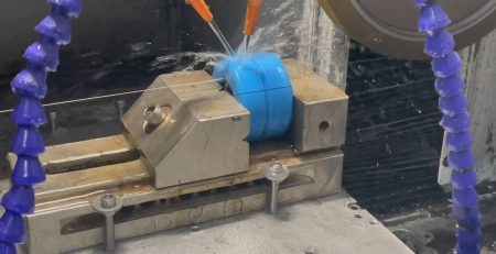
Nel sofisticato mondo della fabbricazione di semiconduttori, Il viaggio da un lingotto di silicio grezzo a un circuito integrato ad alte prestazioni è una meraviglia dell'ingegneria moderna. All'inizio di questo viaggio si trova un processo che definisce l'efficienza dell'intera catena di approvvigionamento:Taglio di wafer di silicio.
Mentre celebriamo il 2026 Festival delle Lanterne e guardiamo a un anno di “Migliore” produzione, Ensoll è orgogliosa di guidare l'innovazione nelle soluzioni di taglio ad alta precisione. Per i produttori, la scelta dell'utensile da taglio non è più solo una decisione di approvvigionamento—è una mossa strategica che determina la resa, i costi, e la competitività globale.
L'intero processo di taglio con sega a filo diamantato — dall'installazione del lingotto alla pulizia della wafer — è documentato passo dopo passo nella nostra guida al silicio monocristallino.
1. Il Ruolo Critico del Taglio delle Wafer di Silicio
Il silicio rimane il “fondamento” dell'era digitale. Whether it is Monocrystalline Silicon for high-efficiency CPUs or Polycrystalline Silicon for solar arrays, the goal of slicing is always the same: to produce thin, flat, and damage-free wafers with the least amount of material loss.
The Challenge of “The Kerf”
In the semiconductor industry, silicon is essentially “liquid gold.” When an ingot is sliced, the thickness of the cutting tool creates a gap called the kerf. The material in this gap is turned into fine dust (trucioli) and lost forever. Traditional sawing methods often lose up to 30% A 40% of the ingot to kerf loss.
gli strumentiSega a filo diamantatotechnology addresses this head-on. By utilizing ultra-thin wires (as thin as 80μm to 120μm), we minimize the “gap” and maximize the number of wafers harvested from a single ingot.
Vetrina video: High-Speed Silicon Slicing
2. Why Diamond Wire Saw Outperforms Traditional Methods
For decades, the industry relied on Slurry Wire Saws (using loose silicon carbide grit in a liquid carrier). Tuttavia, as we move into 2026, DWS has become the undisputed champion. Ecco perché:
Un. Fixed Abrasive Efficiency
In a slurry saw, the grit “rolls” between the wire and the silicon, leading to a chaotic and slow cutting action. In an Ensoll Diamond Wire, the diamonds are electroplated directly onto the wire. Questo “fixed abrasive” method allows for:
Faster Linear Speeds: Reducing cutting time by up to 75%.
Lower Cutting Force: Minimizing the risk of wafer breakage.
B. Superior Surface Geometry
Semiconductor wafers must be perfectly flat. Any “bow” or “deformazione” can cause errors during the subsequent lithography process. Le seghe a filo di Ensoll offrono:
TTV senza pari (Variazione dello spessore totale): Garantendo che ogni wafer sia uniforme dal bordo al centro.
Segni della sega ridotti: Una superficie più liscia significa meno tempo speso nella costosa fase di lucidatura chimico-meccanica (CMP) fase.
Galleria di immagini: Confronto qualità della superficie
3. Il cuore tecnico di Ensoll: La nostra costruzione di filo diamantato.
Non tutti i fili diamantati sono creati uguali. Da Ensoll, il nostro R&Sviluppo ha perfezionato un processo di elettrodeposizione proprietario che garantisce la durata e le prestazioni dei nostri strumenti.
Nucleo ad alta resistenza: Utilizziamo acciaio al carbonio di alta qualità che può sopportare la tensione estrema richiesta per il taglio veloce dei wafer senza rompersi.
Selezione delle particelle diamantate: Utilizziamo diamanti sintetici con forme cristalline specifiche per garantire la massima “presa” nel silicio.
Distribuzione uniforme: Nostro “Migliore” 2026 manufacturing line ensures that diamond particles are distributed with mathematical precision, prevenendo “bald spots” on the wire that cause uneven cuts.
4. Expanding Beyond Silicon: SiC e GaN
The semiconductor landscape is shifting toward Wide Bandgap (WBG) materials like Silicon Carbide (Sic). These materials are nearly as hard as diamond itself, making them notoriously difficult to cut.
Ensoll’s diamond wire saw tools are specifically engineered for these “duri e fragili” challenges. By optimizing the bond between the diamond and the wire, we allow for the efficient slicing of SiC ingots, which is crucial for the burgeoning Electric Vehicle (VE) and 5G Power industries.
5. Environmental and Economic Impact: The Green Advantage
Sustainability is a core pillar of Ensoll’s 2026 mission. La segatura tradizionale a fanghi produce grandi quantità di rifiuti tossici difficili da riciclare.
Zero Slurry: DWS utilizza refrigeranti a base acqua che sono significativamente più facili da filtrare e riciclare.
Efficienza Energetica: Tempi di taglio più rapidi significano un consumo energetico inferiore per wafer.
Riduzione dei Costi: Riducendo la perdita di truciolo e il tempo di lucidatura, Ensoll aiuta i produttori a ridurre significativamente il loro Costo Per Wafer.
6. gli strumenti 2026 Garanzia di Servizio: Le Nostre Tre Promesse
Come evidenziato nell'inizio del nostro Festival delle Lanterne, non stiamo solo fornendo strumenti; stiamo fornendo un “Appagamento” package:
Appagamento di Precisione: Garantiamo che i nostri fili manterranno diametri costanti durante tutta la loro vita utile, garantendo rese stabili.
Esecuzione del Servizio: Il nostro team globale di risposta 4 ore è attivo in ogni principale hub tecnologico (da Singapore agli UAE) per risolvere problemi e ottimizzare le vostre linee.
Partnership Fulfillment: We work with your engineers to customize wire specifications for your specific ingot sizes and machine types.
Silicon wafer cutting is the first cost-defining step in semiconductor fabrication: kerf loss directly sets how many wafers one ingot yields.
Diamond wire saw outperforms ID blades and slurry saws because fixed diamond abrasive gives a narrower kerf, better surface geometry and less material waste.
Ensoll diamond wire combines electroplated diamond grit with high-tensile steel wire, keeping tension stable and wire life long in production slicing.
The same diamond wire platform extends beyond silicon to SiC and GaN substrates with adjusted speed, tension and coolant parameters.
Conclusione: Il “Migliore” Way to Cut
The semiconductor industry moves at light speed, and your cutting technology must keep pace. Silicon Wafer Cutting is the foundation upon which all modern technology is built. By partnering with Ensoll and utilizing our advanced Diamond Wire Saw solutions, you are choosing a path of higher efficiency, lower waste, and superior precision.
As we light the lanterns for 2026, let us light the way for your production line. Experience the “Appagamento di Precisione” that only Ensoll can provide.
Domande Frequenti
Why is diamond wire saw the standard for silicon wafer cutting?
Fixed diamond abrasive cuts with a narrow kerf (tipicamente 120-250 µm), holds tight TTV and wastes far less silicon than ID blades or slurry sawing, so more wafers are produced per ingot.
What is kerf loss and why does it matter?
Kerf loss is the width of material removed by the cut. Every micrometer saved means more wafers per ingot, which is the dominant cost lever in silicon wafer production.
Can the same diamond wire saw cut SiC and GaN?
Sì. Diamond wire handles hard, brittle materials well; only process parameters such as wire speed, tension and coolant need to be adjusted for each material.
What surface quality does diamond wire cutting achieve?
As-cut surfaces typically reach Ra 0.2-0.5 µm with minimal sub-surface damage, which shortens downstream lapping and polishing time.
Contenuto tecnico esaminato dal team di ingegneria Ensoll — un produttore di anelli diamantati con 10+ anni di esperienza produttiva.
Ultima revisione: Settembre 2026
Key Takeaways
Graphite is soft but brittle and abrasive — it dulls blades fast and produces conductive dust,... leggi di più
Legni pregiati come il palissandro e lo huanghuali sono molto ricercati per la loro rarità, Texture unica, e colore. Per massimizzare il... leggi di più
Introduzione alle soluzioni avanzate per il taglio del vetro
Nell'odierno panorama esigente della produzione ottica, taglio con sega a filo diamantato è emerso come l'oro.... leggi di più
Che cosa filo diamantato ciclo?
L'anello del filo diamantato si riferisce a un utensile da taglio costituito da un filo a forma di anello incorporato con diamante.. leggi di più
Nel panorama in continua evoluzione della produzione avanzata, Anello di filo diamantato Il taglio si è affermato come una tecnologia trasformativa per... leggi di più
Magneti al neodimio, conosciuto anche come magneti NdFeB, possiedono una forza incredibile e sono ampiamente utilizzati in una varietà di applicazioni. Tuttavia,... leggi di più
Punti chiave
I fili diamantati scorrono sul vetro con una superficie di taglio rivestita di diamante, permettendo agli artigiani di scolpire bottiglie di birra in design intricati... leggi di più
Punti principali
L'allumina è dura, resistente all'usura e fragile; lo scheggiamento all'ingresso e all'uscita del taglio è il difetto principale... leggi di più
Il taglio a filo diamantato possiede diversi vantaggi significativi nel campo della lavorazione di materiali magnetici, rendendolo un taglio ideale... leggi di più