단결정 실리콘 잉곳 가공 흐름
- A single-crystal silicon ingot goes through cropping, 직경 연삭, 깔 끔 히, 모서리 모서리 캐핑, lapping and polishing before it is ready for lithography.
- Surface accuracy at the slicing stage determines how much downstream planarization work is required.
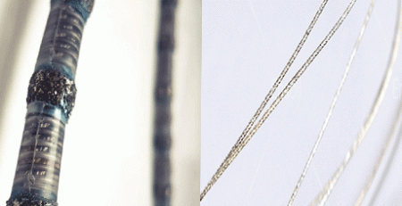
- Diamond wire slicing is the standard way to turn an ingot into bare wafers with tight thickness variation and low sub-surface damage.
단결정 실리콘 웨이퍼 준비 단계에서, 실리콘 단결정 잉곳은 IC 공정의 전반부에서 리소그래피 및 기타 공정을 위한 평탄화를 준비하기 위해 표면 정확도가 높고 표면 품질이 높은 원시 실리콘 웨이퍼 또는 베어웨어로 가공해야 합니다. 여기에는 매우 매끄럽고 손상이 없는 기판 표면이 필요합니다.
직경이 ≤200mm인 실리콘 웨이퍼용, 전통적인 실리콘 웨이퍼 가공 공정은 다음과 같습니다.:
단결정 성장 → 자르기, → 외경, 배럴 연삭, → 플랫 엣지 또는 V-홈 처리, → 웨이퍼링 → 모따기, → 연삭 → 에칭 → 연마 → 세척 → 포장 .

외경 연삭: Since the outer diameter surface of the single crystal silicon rod is not flat and the diameter is larger than the specified diameter specification of the final polished wafer, 외경 압연으로 더 정확한 직경을 얻을 수 있습니다..
플랫 엣지 또는 V-그루브 가공: 참조 평면까지 처리되도록 지정됩니다, and the flat edge or V-groove with a specific crystallographic direction on the 단결정 실리콘 holder.
웨이퍼링: 단결정 실리콘 막대를 정확한 기하학적 치수를 가진 얇은 조각으로 절단하는 것을 말합니다.
깎아 내: 칩 엣지 균열 및 품질 결함을 방지하기 위해 절단된 웨이퍼의 날카로운 모서리를 아크 모양으로 트리밍하는 것을 말합니다
연 삭: 슬라이싱으로 인한 톱 자국 및 표면 손상 층을 제거하고 연삭에 의한 휠 연삭을 말합니다., 휨을 효과적으로 변경, single-product silicon wafer의 평탄도와 평행도, 연마 공정으로 처리할 수 있는 사양에 도달합니다.
자주 묻는 질문
What are the main steps in single-crystal silicon ingot processing?
The typical flow is cropping to length, grinding to precise diameter, slicing into wafers, 모서리 모서리 캐핑, then lapping, etching and polishing to reach the surface quality lithography requires.
Why is slicing done with diamond wire?
Diamond wire gives a narrow kerf, low mechanical damage and high yield per ingot, which keeps both material loss and downstream planarization cost low.
What is a bare wafer?
A bare wafer is the as-sliced wafer before final polishing or epitaxy. It must already meet strict surface accuracy and flatness specifications.
엔솔 엔지니어링 팀이 검토한 기술 내용 — 다이아몬드 와이어 루프 제조업체 10+ 다년간의 생산 경험을 가진 회사.