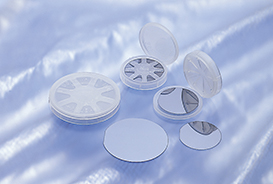
Un chip semiconductor, comúnmente conocido como circuito integrado, es un dispositivo semiconductor fabricado en una oblea de semiconductor mediante procesos como grabado, cableado, y modelado para lograr funciones específicas. Más allá de los chips de silicio, los materiales semiconductores comunes incluyen arseniuro de galio, nitruro de galio, y carburo de silicio.
Última revisión: Septiembre 2026
Puntos clave
Los semiconductores son materiales con conductividad entre conductores y aislantes, formando la base de todos los circuitos integrados.
Más allá del silicio, los tipos clave de semiconductores incluyen arseniuro de galio (Gaas), nitruro de galio (Gan) y carburo de silicio (Sic), cada uno con nichos de aplicación distintos.
GaAs sirve para RF y optoelectrónica, GaN sirve para potencia de alta frecuencia, y SiC sirve para dispositivos de potencia de alto voltaje, alta temperatura.
El proceso de fabricación de semiconductores es similar a convertir materiales básicos en oro, implicando principalmente una serie de tratamientos en obleas de silicio. En esencia, a través de crecimiento epitaxial, fotolitografía, etching, dopado, y pulido, los circuitos requeridos se forman en la oblea de silicio, transformándola en un chip.
Tipos de semiconductores
Los materiales semiconductores son materiales electrónicos utilizados en la producción de dispositivos semiconductores y circuitos integrados, formando la base de la industria de semiconductores.
Con la aparición de nuevos materiales semiconductores, avances en la tecnología de la electrónica de potencia, y mejoras en los procesos de fabricación, los semiconductores han pasado por tres generaciones de cambios. Arseniuro de galio (Gaas) y nitruro de galio (Gan), así como carburo de silicio (Sic) semiconductores, representan la segunda y tercera generación de semiconductores, respectivamente.
En comparación con el silicio, semiconductor de primera generación (Si), estos materiales muestran un rendimiento superior en aspectos como alta frecuencia y alta temperatura.
Los chips de semiconductores compuestos, conocidos por su excelente rendimiento en alta frecuencia, se utilizan comúnmente en la producción de semiconductores de potencia, con sus aplicaciones volviéndose cada vez más extendidas. A través de técnicas como la conversión de frecuencia, transformación de voltaje, modulación de corriente, amplificación de potencia, y gestión, estos chips cumplen dos funciones principales: amplificación y conmutación.
Actualmente, sobre 75% las aplicaciones de energía requieren conversión de potencia antes de ser suministradas a los dispositivos. Sus aplicaciones continúan expandiéndose.
La amplificación implica convertir potencia de baja frecuencia en potencia de alta frecuencia, aprovechando la amplificación para accionar motores con poca potencia de manera eficiente. La conmutación consiste en alternar los circuitos encendidos y apagados, con velocidades de conmutación más rápidas que permiten un control preciso.
Amplificación: Convertir potencia de baja frecuencia en potencia de alta frecuencia, hacer pleno uso de la amplificación permite accionar motores con poca potencia de manera efectiva.
Conmutación: Alternar el circuito encendido y apagado, cuanto mayor sea la velocidad de conmutación, más preciso se puede lograr el control.
Semiconductor de Arseniuro de Galio
Los chips de semiconductor de arseniuro de galio se utilizan principalmente en dispositivos de potencia de microondas, que operan en el rango de frecuencia de microondas (entre 300 y 300,000 megahercios). Debido a las limitaciones físicas inherentes al silicio (Si), solo se puede aplicar a frecuencias por debajo de 1 GHz. Sin embargo, en los últimos años, el rápido desarrollo de productos de comunicación inalámbrica de alta frecuencia ha impulsado al arseniuro de galio al frente, mostrando características como altas frecuencias de operación, tasas de movilidad de electrones, resistencia a la radiación natural, y bajo consumo de energía, lo que lo hace ampliamente utilizado en el campo de la comunicación por microondas.
Dadas las características de transmisión de alta frecuencia del arseniuro de galio, ha experimentado un crecimiento rápido no solo en aplicaciones de teléfonos móviles, sino también en módulos WiFi integrados en portátiles, tabletas, transmisión inalámbrica de redes fijas, así como en comunicación por fibra óptica, comunicación por satélite, comunicación punto a punto por microondas, televisión por cable, sistemas de navegación automotriz, y sistemas de evitación de colisiones. Estas aplicaciones a menudo emplean diferentes cantidades de amplificadores de potencia (que van desde 1 Para 4 chips), impulsando el avance significativo del arseniuro de galio.
Semiconductor de Nitruro de Galio
Material de nitruro de galio, con un ancho de banda de 3.4 eV, se considera un material semiconductor de tercera generación junto con materiales como SiC y diamante, conocidos como semiconductores de banda ancha. Debido a sus ventajas como un ancho de banda amplio, alto campo de ruptura, gran velocidad de saturación de electrones, Alta conductividad térmica, Baja constante dieléctrica, Estabilidad química, y fuerte resistencia a la radiación, el nitruro de galio se ha convertido en uno de los materiales preferidos para alta temperatura, alta frecuencia, y dispositivos de microondas de alta potencia.
Comparación del nitruro de galio (Gan) con arseniuro de galio (Gaas) y silicio (Si):
La creciente demanda de dispositivos semiconductores de alta velocidad, alta temperatura, y alta potencia ha llevado a la adopción gradual del material de nitruro de galio en el mercado de semiconductores. Sus principales áreas de aplicación incluyen:
Sector de Energía Renovable:
En el campo de la energía renovable, el nitruro de galio desempeña un papel extremadamente importante en la integración de la energía eólica y solar en la red y en la reducción de pérdidas de transmisión. Energía verde, los vehículos eléctricos, iluminación electrónica verde, y otras áreas emergentes se están convirtiendo en nuevos puntos calientes para las aplicaciones del mercado de dispositivos de potencia, con fuerte demanda.
Sector de Equipos de Información y Comunicación:
Los transistores mejorados de nitruro de galio exhiben alta resistencia a la radiación, making them suitable for power and communication systems in communication and scientific satellites. Point-to-point communication, comunicación por satélite, various radars, and new industrial/defense applications will benefit from the application of these high-power gallium nitride devices.
4C Industries:
Major domestic IT products are expected to maintain strong market demand, with traditional products like laptops, monitors, printers, televisions, home theater systems, and Blu-ray players, as well as emerging automotive electronics, projected to experience steady growth in the future. As production capacity for electronic products such as air conditioners and energy-efficient motors shifts to the Chinese mainland, the demand for power semiconductors is expected to double.
Smart Grid Sector:
Power semiconductors play a crucial role in improving the overall energy efficiency of the entire power supply chain—from generation, transmission, and distribution to end-user consumption—in the field of smart grids.
Silicon Carbide Semiconductor
Carburo de silicio (Sic) has become one of the most prominent semiconductor materials due to its outstanding performance under high temperature, Alta presión, and high frequency conditions. It is widely used in power conversion devices such as AC-DC converters and is expected to gradually replace silicon comprehensively in the field of semiconductor power devices, heralding the dawn of the Silicon Carbide Semiconductor era.
Compared to silicon devices, SiC semiconductor chips can reduce power losses by nearly 50%, effectively enhancing power conversion efficiency. SiC devices, with their high conversion efficiency and low heat generation, can reduce the size of cooling systems, leading to overall downsizing of power conversion devices. This is of significant importance for systems like new energy vehicles that require numerous power conversion devices. Por lo tanto, for systems requiring high conversion efficiency and power density, SiC devices offer unparalleled advantages and are the preferred choice.
Due to its exceptional performance, silicon carbide is particularly suitable for applications requiring high-power conversion, such as deep well drilling, solar inverters (for DC to AC conversion), wind energy inverters, electric and hybrid vehicles, industrial drives, and light rail traction systems.
Fabrication Method:
The semiconductor manufacturing process is akin to turning lead into gold, implicando principalmente una serie de tratamientos en obleas de silicio. While a detailed explanation can be quite complex, in simple terms, it involves epitaxial growth, fotolitografía, etching, dopado, and polishing to create the required circuits on the silicon wafer, transformándola en un chip. Steps like photolithography and etching still rely on foreign technologies and the use of foreign patents
Semiconductor processing methods
Four Cutting Technologies: A Comparative Overview:
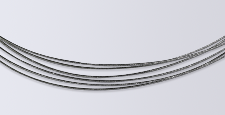
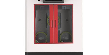
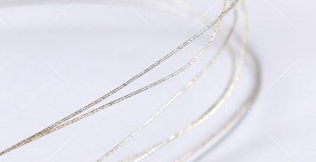
1. Corte con bucle de hilo de diamante
Principle: A fast-moving loop of wire, recubierto con partículas de diamante, acts as a cutting tool, grinding through the material. Coolant is often used.
Key Advantage:Low stress, Alta precisión, desperdicio mínimo de material. El “flexible” wire is gentle on brittle materials, enabling clean cuts with almost no edge chipping. It is the preferred method for slicing high-value, duro, brittle materials like SiC, Gan, zafiro, y vidrio ópticointo thin wafers.
Limitation:Limited cutting speed. As a grinding process, its material removal rate is slower than thermal methods like laser cutting, making it less efficient for high-volume or rough cutting jobs.
2. Diamond Saw Blade Cutting
Principle:A rotating circular blade with a diamond-coated edge cuts through the material, similar to a precision stone cutter.
Key Advantage:Proven technology, Alta eficiencia, relatively low cost. It’s the standard method for rough cutting and sizing blocks of silicon and ceramic.
Limitation:High mechanical impact. It can easily cause edge chipping and internal stress or micro-cracks, making it unsuitable for finishing ultra-thin, ultra-hard, or high-value materials.
3. Corte por láser
Principle:A focused, high-energy laser beam melts, vaporizes, or alters the material, with a gas jet removing the debris.
Key Advantage:Non-contact, no tool wear, very fast, highly flexible. It easily handles complex 2D shapes and can perform “stealth dicing” (separación mediante modificación interna), lo que lo hace ideal para el corte de obleas y el conformado de silicio, zafiro, y vidrio.
Limitation: Crea una zona afectada por el calor que puede cambiar las propiedades del material en el borde cortado. Puede tener dificultades con materiales altamente reflectantes (p ej., cobre puro) o materiales transparentes. El equipo es caro.
4. Corte por descarga eléctrica (Electroerosión por hilo)
Principle: Descargas de chispa controladas entre un electrodo de alambre delgado y la pieza de trabajo generan calor intenso, fundiendo y vaporizando el material localmente.
Key Advantage: Corta cualquier material conductor sin importar la dureza (p ej., acero endurecido, carburo de tungsteno, cerámicas conductoras). Alcanza una precisión muy alta y puede crear formas complejas.
Limitation: Solo funciona con materiales conductores. El proceso es lento, y deja una capa reprocesada en la superficie cortada.
Resumen & Guía de selección
No existe una única “mejor” tecnología: cada una es más adecuada para tareas específicas:
For ultimate cut quality and minimal loss when slicing hard, brittle wafers (p ej., Sic): ChooseBucle de alambre de diamante Cortante.
For efficient, corte tosco de bajo costo de bloques duros, frágiles: Elija la hoja de sierra de diamante para cortar.
Para corte de alta velocidad de formas 2D complejas en varios materiales (incluidos los no metálicos): Elija corte por láser.
Para mecanizar formas intrincadas en materiales muy duros, conductores (p ej., moldes): El corte por descarga eléctrica es la única opción.
Situación actual:
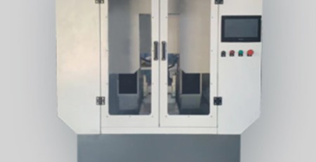
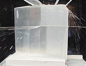
Actualmente, muchas tecnologías requieren que se les infunda una perspectiva más fresca, ya que cada paso del proceso podría potencialmente conducir a avances significativos. Con respecto a un aspecto específico, realizamos un experimento cortando lingotes de 12 pulgadas hace dos semanas. UtilizamosEnsolltoolsLimited’s sierra de alambre de diamante Tecnología, donde las marcas del alambre son casi invisibles, y la planitud se puede controlar dentro de 3 micrones. Este método aborda muchos problemas relacionados con el corte de superficies cóncavas de semiconductores, reduciendo en gran medida la dificultad del pulido posterior y el consumo de material.
Sea cual sea el tipo de semiconductor involucrado, los dispositivos aún comienzan su vida en el proceso de corte de obleas.
Preguntas Frecuentes
Qué es un semiconductor?
Un semiconductor es un material cuya conductividad eléctrica se sitúa entre un conductor y un aislante y puede ser controlada mediante dopado, lo que lo convierte en la base de los circuitos integrados.
Cuáles son los principales tipos de materiales semiconductores?
El silicio domina los circuitos integrados generales; Los semiconductores compuestos incluyen arseniuro de galio (RF, optoelectrónica), nitruro de galio (potencia de alta frecuencia) y carburo de silicio (de alta tensión, potencia a alta temperatura).
Dónde se utilizan los semiconductores SiC y GaN?
El SiC se utiliza en inversores de vehículos eléctricos y módulos de potencia de alta tensión, mientras que el GaN se utiliza en cargadores rápidos, amplificadores de potencia RF e infraestructura 5G.
Contenido técnico revisado por el equipo de ingeniería de Ensoll — un fabricante de bucles de hilo de diamante con 10+ años de experiencia en producción.
Bucles de alambre de diamante representan un pináculo de precisión en el ámbito de las herramientas de corte, aprovechando la extraordinaria dureza de... . leer más
En el exigente mundo de los semiconductores avanzados, donde el rendimiento y la eficiencia son primordiales, un material se destaca como un habilitador crítico:... leer más
Puntos clave
La guía de corte con alambre de diamante utiliza un alambre recubierto de diamante enrollado en un lazo sin interrupciones sobre la superficie de la lente, escultura intrincada.... leer más
Puntos clave
Un semiconductor es un material con propiedades entre un aislante y un conductor, controlable mediante dopaje y campos eléctricos.
Comprensión... leer más
Abstracto: Este informe de aplicación documenta una prueba de corte recto de alta precisión en lámina de vidrio BG38 suministrada por un cliente europeo. La pieza de trabajo medida.... leer más
En el mundo sofisticado de la fabricación de semiconductores, el viaje desde un lingote de silicio crudo hasta un circuito integrado de alto rendimiento es... leer más
Bucles de alambre de diamante se fabrican utilizando procesos avanzados de manufactura donde los diamantes se incrustan en un bucle de hilo. Éste... leer más