Laser vs scie à fil diamanté pour le carbure de silicium
Dans le monde des matériaux avancés, découpage carbure de silicium (Sic) présente des défis uniques qui exigent des solutions spécialisées. En tant que matériau semi-conducteur de troisième génération, le carbure de silicium possède des propriétés exceptionnelles, notamment une dureté extrême (9.5 Mohs, seconde seulement au diamant), une haute résistance thermique, et une inertie chimique . Ces mêmes caractéristiques qui rendent le SiC précieux pour l'électronique de puissance, Véhicules électriques, et les applications aérospatiales le rendent également notoirement difficile à traiter. Avec le marché mondial du SiC en expansion rapide, principalement driven par l'adoption des véhicules électriques et les technologies d'énergie renouvelable, l'importance de méthodes de découpe efficaces, et précises n'a jamais été aussi grande .
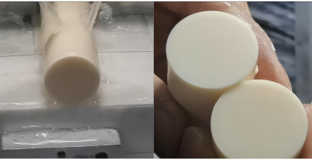
La dureté en soi n'est pas unique au SiC – la même contrainte s'applique Découpe de céramiques en alumine, quoique pour des raisons différentes.
- L'extrême dureté du carbure de silicium rend le choix de la méthode critique: le laser est rapide mais crée une zone affectée par la chaleur, la scie à fil diamant coupe à froid avec une qualité de surface supérieure.
- La scie à fil diamant produit moins de dommages sous la surface, réduction du post-traitement pour les plaquettes et pièces en SiC.
- Pour les SiC épais et les exigences de précision, la boucle de fil diamanté est le choix de production le plus sûr.
le choix d'outils de coupe en carbure de silicium appropriés impacte directement l'efficacité de fabrication, la qualité du produit, et les coûts de production. Actuellement, deux méthodes principales sont apparues comme les meilleures options pour le traitement du SiC: la découpe laser et scie à fil diamanté découpage. Chaque approche offre des avantages et des limites distincts, les rendant adaptées à différentes applications et scénarios de production. Cette analyse complète examine les deux technologies pour aider les fabricants et ingénieurs à prendre des décisions éclairées sur leurs stratégies de traitement du SiC.
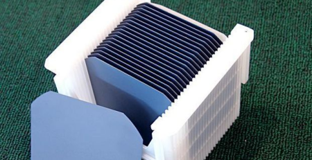
Le choix de la même méthode détermine le rendement dans la découpe de plaquettes de silicium, où il a été décidé des années auparavant à l'échelle de la production.
Pour le côté outillage de la coupe du carbure de silicium — diamètre du fil, grain et tension — voir notre guide dédié.
Comprendre la découpe au fil diamanté pour le carbure de silicium
La technologie derrière la découpe au fil diamanté
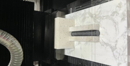
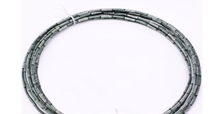
Scie à fil diamanté la découpe représente une évolution des méthodes traditionnelles de découpe au fil, en utilisant une boucle continue de fil incrustée de particules de diamant pour trancher à travers le matériau SiC par action de broyage mécanique . Le mécanisme fondamental implique un fil à grande vitesse recouvert de particules de diamant se déplaçant à travers la pièce en SiC, avec les particules de diamant agissant comme des outils de coupe microscopiques qui abrasent progressivement le matériau.
Cette forme en boucle fermée est ce qui distingue un boucle de fil de diamant d'une scie à fil enroulée sur bobine.
Le processus de découpe relève de la catégorie de “traitement à deux corps,” où les particules de diamant fixes s'engagent directement avec le matériau de la pièce . Cela diffère considérablement des méthodes traditionnelles à base de boue qui s'appuient sur “traitement à trois corps” avec des particules abrasives libres. La configuration du fil diamant permet un enlèvement de matière plus efficace tout en maintenant un contrôle précis des paramètres de coupe.
Avantages de la découpe à la scie à fil diamanté
La technologie du fil diamant offre plusieurs avantages convaincants pour la découpe du carbure de silicium:
- Vitesse et efficacité de coupe supérieures: Les scies à fil diamant atteignent des vitesses de coupe nettement plus rapides par rapport aux méthodes traditionnelles, en particulier lors du traitement de grands cristaux de SiC . Le mouvement continu du fil imprégné de diamant permet un enlèvement de matière efficace, réduisant le temps de traitement global dans les environnements de production à haut volume. En réalisant que la vitesse dépend de la machine, et notre machine de découpe de scie à fil diamanté aperçu compare les architectures qui la sous-tendent.
- Haute précision avec perte de trait minimale: La technologie offre une excellente précision de coupe avec un gaspillage de matériau relativement minimal . Alors que la largeur de coupe (matériau retiré lors de la coupe) varie typiquement de 120 à 200 μm , cela représente une amélioration par rapport aux méthodes traditionnelles à base de suspension abrasive et aide à conserver le matériau SiC coûteux.
- Scalabilité prouvée pour les applications industrielles: La découpe avec fil diamanté s'est imposée comme la technologie de tranchage dominante pour les plaquettes de silicium dans la fabrication photovoltaïque . Cette validation industrielle démontre son adéquation pour des environnements de production à haut volume où la cohérence et le débit sont essentiels. Le détail du processus derrière cette dominance est présenté dans notre la découpe de plaquettes de silicium guide. (lien 2 de 2)
- Impact environnemental réduit: Les systèmes modernes à fil diamanté éliminent ou réduisent significativement le besoin de suspensions abrasives, aborder les défis liés à l'élimination des déchets associés à la découpe traditionnelle à l'eau de coupe . Cet avantage environnemental s'aligne sur des réglementations de fabrication de plus en plus strictes.
Limites de la découpe au fil diamanté
Malgré ses avantages, La découpe au fil diamanté présente plusieurs limitations importantes:
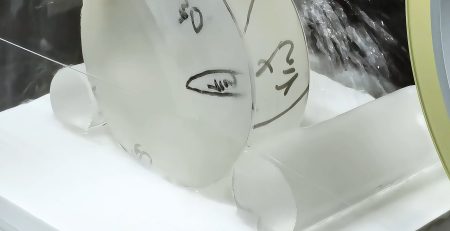
- Dommages en surface et en sous-surface: La nature mécanique de la découpe au fil diamanté génère une couche de dommages épaisse qui nécessite souvent un polissage ou une gravure ultérieure pour restaurer la qualité de la surface . Ce traitement supplémentaire ajoute du temps et des coûts au flux de fabrication. La profondeur des dommages est tout aussi importante pour les substrats transparents, comme les tolérances pour découpe optique du verre clarifier.
- Défis de gestion thermique: Le processus de découpe génère une chaleur importante, ce qui peut provoquer des dommages thermiques sur la pièce en SiC si elle n'est pas correctement contrôlée . Effective cooling systems are essential to mitigate this risk, adding complexity to the equipment.
- Material Utilization Concerns: While improved over slurry methods, diamond wire cutting still results in material loss up to 46% in some applications . This represents substantial waste of expensive SiC material, directly impacting production economics. How much of that loss is recoverable depends on the configuration, which is why our comparison of single-wire and multi-wire diamond wire cutting separates the two cases.
- Geometric Limitations: Diamond wire cutting is primarily suited for straight cuts and standardized geometric patterns, with limited capability for complex contours or intricate shapes .
Understanding Laser Cutting for Silicon Carbide
The Technology Behind Laser Cutting
Laser cutting represents a non-contact thermal processing method that utilizes a high-energy laser beam to melt, vaporize, or ablate SiC material in a precisely controlled manner . Different laser types, including ultraviolet, picosecond, femtosecond, and nanosecond lasers, offer varying capabilities for SiC processing .
Heat input is the failure mechanism to watch, a point made concrete by the recast layers seen in precision ZnSe cutting.
The fundamental mechanism involves focusing a high-energy radiation beam onto a small-diameter spot on the SiC surface, creating rapid, high-temperature-gradient heating that triggers material removal . Advanced systems often incorporate gas assist to blow away melted/vaporized material and expose fresh surface for continued cutting.
Les récentes innovations technologiques ont élargi les capacités des lasers pour le traitement du SiC:
– Découpe laser guidée par l'eau: Également connue sous le nom de technologie Laser MicroJet, cette approche utilise un jet d'eau pressurisé pour guider le faisceau laser vers la pièce, fournissant simultanément refroidissement et évacuation des débris .
– Découpe discrète: Cette technique concentre le faisceau laser sous la surface du matériau pour créer une couche modifiée, permettant une séparation précise avec des dommages minimaux à la surface .
– Traitement laser ultrarapide: Les lasers femtosecondes et picosecondes permettent un traitement de matériau extrêmement précis avec des dommages thermiques minimes grâce à leurs durées d'impulsion ultracourtes .
Avantages de la découpe laser
La technologie laser offre plusieurs avantages distincts pour la découpe du carbure de silicium:
- Précision et flexibilité exceptionnelles: La découpe au laser permet des designs extrêmement complexes et des géométries compliquées qui seraient difficiles ou impossibles avec des méthodes mécaniques . La nature sans contact du processus permet de couper sans appliquer de force physique sur la pièce.
- Dommages mécaniques minimaux: Contrairement aux méthodes mécaniques, la découpe au laser élimine des problèmes tels que l'usure des outils, le stress mécanique, et les dommages induits par les vibrations . Cela se traduit par des découpes de meilleure qualité avec une réduction des micro-fissures dans le matériau fragile SiC.
- Utilisation supérieure du matériau: Les méthodes au laser réduisent considérablement la perte de matériau par rapport aux approches mécaniques. La recherche indique que le même lingot de SiC peut produire 50% plus de plaquettes avec la découpe au laser par rapport aux méthodes de sciage à fil . Certaines techniques laser avancées revendiquent une découpe presque sans perte avec une utilisation du matériau approchant 100% .
- Impact thermique réduit grâce aux lasers avancés: Lasers ultrarapides (femtoseconde et picoseconde) générer des zones affectées par la chaleur minimales, préservant les propriétés matérielles du SiC et réduisant les besoins de traitement ultérieurs .
Limitations de la découpe laser
Malgré ses avantages prometteurs, la technologie de découpe laser fait face à plusieurs défis:
- Coûts élevés d'équipement et d'exploitation: Les systèmes de découpe laser représentent des investissements en capital substantiels, avec des systèmes sophistiqués allant de $10,000 À $150,000 ou plus . La maintenance et l'exploitation nécessitent une expertise spécialisée, ce qui augmente les dépenses opérationnelles. Le coût en capital n'est qu'une partie de la comparaison – le coût par découpe est là où la machine de découpe à fil diamant ESC600 tend à être meilleure sur les sections épaisses.
- Limitations de débit: Tout en excellant en précision, la découpe laser offre généralement un débit inférieur par rapport aux scies multi-fils diamantées pour une production à grand volume . Cela le rend moins adapté aux applications où la vitesse de production est la principale préoccupation.
- Complexité technique: Le traitement laser du SiC nécessite une optimisation soigneuse des paramètres pour obtenir les résultats désirés sans provoquer de dommages thermiques, y compris la durée de l'impulsion, la longueur d'onde, la densité d'énergie, et la vitesse de balayage .
- Limitations d'épaisseur: L'efficacité de la découpe laser diminue avec l'épaisseur du matériau, ce qui le rend moins adapté aux substrats SiC très épais par rapport aux méthodes mécaniques .
Comparaison directe: Facteurs de performance critiques
Qualité de coupe et intégrité de la surface
Lors de l'évaluation des outils de découpe du carbure de silicium, la qualité finale de la pièce est une considération primaire. La découpe à la scie à fil diamant produit généralement des surfaces avec des dommages sous-jacents plus importants, y compris des microfissures et des marques de scie nécessitant un polissage ultérieur important . La contrainte mécanique exercée lors de la découpe peut compromettre l'intégrité structurelle des fines plaquettes.
La découpe au laser produit généralement des bords plus propres avec des dommages mécaniques minimes, mais introduit des effets thermiques pouvant modifier les propriétés du matériau. Des études montrent que l'ablation au laser peut réduire la dureté de surface à moins de 1% des valeurs initiales (en dessous de 50 MPa à partir de la valeur initiale 13,896 Mpa) . Les lasers ultrarapides avancés réduisent significativement ces effets thermiques, mais à un coût d'équipement plus élevé.
Débit de production et efficacité
Pour les environnements de fabrication à grande échelle, le débit de production est un facteur critique. Scies à fil diamanté, en particulier pour les configurations multi-fils, peuvent traiter plusieurs plaquettes simultanément, offrant des avantages significatifs pour la production de masse . Le mouvement de découpe continu et la mise en œuvre industrielle établie permettent un débit élevé pour les tailles de plaquettes standard.
Les systèmes de découpe au laser traitent généralement les plaquettes de manière séquentielle, limitation du débit maximal. Toutefois, pour les géométries complexes ou les applications spécialisées, les lasers peuvent offrir des avantages en termes d'efficacité en combinant plusieurs étapes de traitement ou en réduisant les besoins de polissage ultérieurs.
Économie opérationnelle et considérations de coût
L'analyse économique de la coupe du carbure de silicium doit prendre en compte à la fois l'investissement en capital et les dépenses opérationnelles. Les scies à fil diamanté représentent une technologie mature avec des coûts opérationnels connus, bien que les dépenses en consommables (fils diamantés) et l'élimination des déchets contribuent de manière significative au coût total de possession.
Les systèmes de découpe laser nécessitent un investissement initial plus élevé mais offrent des économies potentielles grâce à la réduction des déchets de matériel et à une meilleure utilisation des matériaux. À mesure que la technologie laser se développe et devient plus répandue, les coûts des équipements devraient diminuer, améliorant la viabilité économique.
Material Versatility and Application Range
Bien que cette analyse se concentre sur la découpe du carbure de silicium, les fabricants traitent souvent plusieurs matériaux. Les scies à fil diamanté démontrent d'excellentes performances sur divers matériaux durs et friables, y compris le silicium, saphir, et les céramiques avancées . Cette polyvalence peut être avantageuse dans les installations traitant plusieurs types de matériaux.
Les systèmes de découpe au laser offrent également une flexibilité des matériaux, avec des ajustements de paramètres permettant le traitement de divers matériaux, des métaux aux composites . Toutefois, L'optimisation pour des matériaux spécifiques comme le SiC peut réduire les performances pour d'autres applications.
Recommandations spécifiques à l'application
Fabrication de semi-conducteurs à grand volume
Pour la production en grande série de tranches standards de SiC pour l'électronique de puissance, la découpe à la scie à fil diamanté offre actuellement le meilleur équilibre entre rendement, et constance, et familiarité opérationnelle . L'infrastructure et les contrôles de processus établis soutiennent les exigences strictes de qualité de la fabrication de semi-conducteurs.
Prototypage et production en faible volume
Pour les institutions de recherche, installations de prototypage, et production en faible volume de composants spécialisés, la découpe laser offre une flexibilité supérieure et des temps de configuration plus rapides . La capacité de mettre en œuvre rapidement des modifications de conception sans modification des outillages rend les lasers idéaux pour les environnements de développement.
Géométrie complexe et composants miniaturisés
Pour les applications nécessitant des formes complexes, contours, ou des fonctionnalités miniaturisées, la découpe laser est sans équivoque supérieure . Le procédé sans contact et le chemin de faisceau programmable permettent des géométries complexes impossibles avec des méthodes mécaniques.
Traitement de sections épaisses et grand format
Pour les substrats SiC épais ou le traitement grand format, diamond wire saws currently maintain advantages in cutting efficiency and established capability . While laser technology continues to advance in this area, mechanical methods remain more practical for very thick materials.
Future Outlook and Technology Trends
The landscape of silicon carbide cutting tools continues to evolve with both technologies advancing rapidly. Diamond wire saw development focuses on finer wires, improved diamond particle distribution, and enhanced tension control systems to reduce kerf loss and improve surface quality .
Laser cutting innovation centers on increased power, improved beam quality, and advanced processing techniques to enhance throughput and reduce thermal effects. Emerging approaches like hybrid processing combine laser pretreatment with mechanical polishing to optimize both efficiency and quality .
Industry analysts project strong growth for both technologies, with the SiC wafer laser cutting equipment market expected to expand significantly through 2033 . As manufacturing volumes increase and technology improves, laser methods are anticipated to capture greater market share, particularly for advanced applications demanding highest precision and minimal material loss.
Conclusion: Selecting the Right Approach for Your Needs
The choice between diamond wire saw cutting and laser cutting for silicon carbide processing involves careful consideration of application requirements, production volume, quality specifications, and economic factors.
Diamond wire saw cutting remains the preferred solution for high-volume production of standard SiC wafers, offering proven reliability, high throughput, and established process controls. Its limitations in surface quality and material utilization are offset by its robustness and predictability in industrial environments.
Laser cutting technology provides compelling advantages for applications prioritizing precision, géométries complexes, and material utilization. While requiring greater capital investment and technical expertise, its capabilities align with industry trends toward thinner wafers, more complex devices, and sustainable manufacturing through reduced material waste.
As SiC continues its expansion into power electronics, Véhicules électriques, and advanced applications, both cutting technologies will evolve to meet increasing demands for precision, efficacité, et une rentabilité. Understanding their respective strengths and limitations enables manufacturers to implement optimal processing strategies for their specific requirements, ultimately supporting the broader adoption of silicon carbide across advanced technology sectors.
Questions fréquemment posées
Is laser or diamond wire saw better for cutting silicon carbide?
Pour les travaux de précision, scie à fil diamanté: it cuts without a heat-affected zone, giving better surface integrity and less sub-surface damage. Laser is faster on thin sections but leaves thermal damage and recast layers.
Why is silicon carbide so hard to cut?
SiC approaches diamond in hardness (Mohs ~9.2-9.5) et est fragile, so mechanical blade sawing causes chipping and laser cutting causes thermal micro-cracks. Diamond abrasive wire is one of the few practical tools.
Does laser cutting damage SiC wafers?
Laser ablation creates a heat-affected zone with micro-cracks and recast material that must be removed by extra grinding, adding cost and yield loss — especially critical for semiconductor-grade SiC.
What surface quality can a diamond wire saw achieve on SiC?
With fine wire and optimized parameters, Ra in the sub-micron range is achievable, often eliminating or reducing lapping before polishing.
Contenu technique examiné par l'équipe d'ingénierie d'Ensoll — un fabricant de boucles de fil diamanté avec 10+ des années d'expérience en production.