Cutting SiC/GaN: How Diamond Wire Saw Solves It

Cutting SiC/GaN: How Diamond Wire Saw Solves It

Key Takeaways

  • SiC and GaN are third-generation semiconductors transforming power electronics, 5G and EVs — but they are extremely hard to cut.
  • Their ultra-high hardness, brittleness and thermal-stress sensitivity defeat most conventional cutting methods.
  • Diamond wire saw solves SiC/GaN cutting with the hardest abrasive in a cold, low-force, narrow-kerf process.

導入

の台頭 第3世代半導体材料 (SiCとGaN) パワーエレクトロニクスを変革しました, 5G, および電気自動車産業. でも, その極端な硬度と脆性により、 精密切断 製造上の大きなハードル. この記事では、 SiC/GaNウェーハの切削課題 でなぜ ダイヤモンドワイヤーソー テクノロジー は最適なソリューションです.

SiC/GaNの切断が難しい理由?

semiconductor691. 超高材料硬度

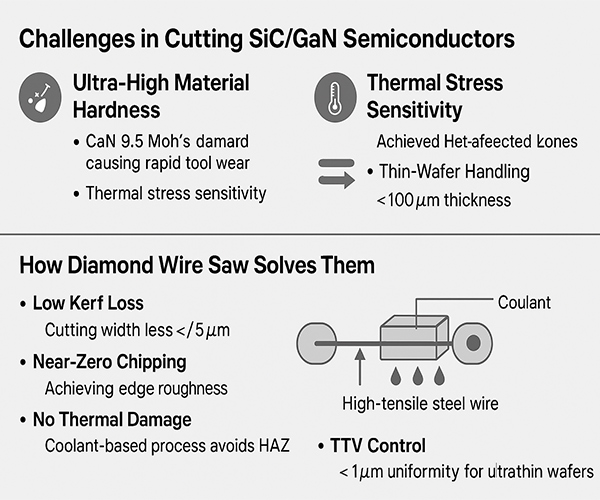
  • ティッカー (炭化ケイ素): 9.5 モース硬度 (ダイヤモンドに近い), 工具の急速な摩耗を引き起こす.
  • GaNの (窒化ガリウム): 高い破壊靭性, マイクロクラックが発生しやすい.

2. 脆性 & エッジチッピング

伝統的な切断方法 (例えば。, ブレードダイシング) 生成する エッジ欠陥 (>20μmチッピング), で歩留まりを減らす パワーデバイス そして RFチップ.

3. 熱応力感度

レーザー切断は、 熱影響部 (ハズ), 高周波アプリケーションにとって重要な材料特性の変更.

4. 薄ウェーハハンドリング

先端パッケージングのためのSiC/GaNウェーハ (例えば。, チップレット設計) 要する <100μmの厚さ サブ1μmTTV付き (総厚変化).

ダイヤモンドワイヤー切断: 最適なソリューション

1. ダイヤモンドワイヤーソーの仕組み

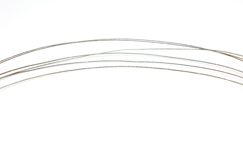
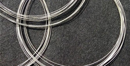
  • 電気めっきダイヤモンド粒子(5-50μm) 高張力鋼線.

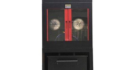
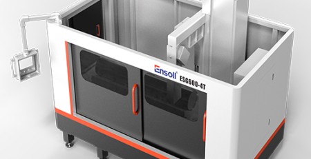
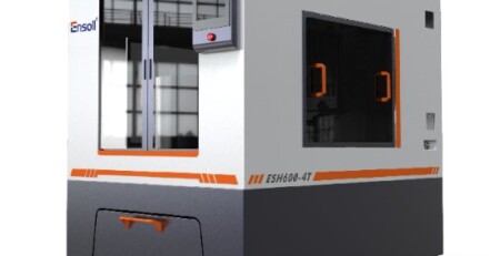
無限のダイヤモンドワイヤーソー 9l ・往復運動、連続運動 冷却剤付きで熱ストレスを最小限に抑制.

2. SiC/GaNの主な利点

  • 低カーフ損失: <50μm切断幅VS. 200μm in ブレードダイシング (材料の節約).
  • ニアゼロチッピング: 実現 <5μmエッジ粗さ (クリティカル HEMTデバイス).
  • 熱による損傷はありません: クーラントベースのプロセスでHAZを回避.
  • TTV制御: <1μmの均一性 極薄ウェーハ.

ケーススタディー: SiCパワーモジュールの製造

半導体大手EVメーカーがレーザーからレーザーに切り替えました。 ダイヤモンドワイヤー切断 SiC MOSFET用:

  • 結果 1: から歩留まりが増加しました 78% 宛先 93%(亀裂による故障の低減).
  • 結果 2: カット速度に到達 500ミリメートル/分0.3μmのダイヤモンドワイヤー付き

適切なダイヤモンドワイヤーソーの選択

SiC/GaNアプリケーション向け, 優先 順位:

  • 線径: 0.1-0.3mmで細かい仕上げ.
  • ダイヤモンドグリットサイズ: 10–20μm 速度と表面品質のバランス.
  • 機械の安定性: 振動 <0.1マイクロクラックを防ぐためのμm.

今後の動向

  • ハイブリッドカッティング: ダイヤモンドワイヤーとレーザープリグルービングの組み合わせにより、 異種混合統合.
  • AIベースのプロセス制御: のリアルタイム調整 欠陥のない切断.

結論

ダイヤモンドワイヤーソー技術は、 硬度, 脆性, と熱の課題 SiC/GaN切断の, 歩留まりの向上とウェーハの薄型化を実現. 半導体メーカー様向け, 投資 精密ダイヤモンドワイヤー装置 次世代デバイスのスケーリングに不可欠.

SiC/GaN切削ソリューションを探しています? お 問い合わせ お客様のニーズに合わせたダイヤモンドワイヤーソーシステムの無料相談.
For a full process walkthrough, see how to process silicon carbide from slicing through to finish.

Frequently Asked Questions

Why are SiC and GaN so difficult to cut?

Both materials combine Mohs 9-class hardness with brittleness and sensitivity to thermal stress, so blades wear fast and lasers risk heat-induced cracks.

How does diamond wire saw solve SiC and GaN cutting?

Diamond abrasive handles the hardness, while the cold, low-force wire process avoids thermal damage and minimizes edge chipping and sub-surface cracks.

What is third-generation semiconductor material?

Wide-bandgap semiconductors such as SiC and GaN that operate at higher voltage, frequency and temperature than silicon, driving power electronics, 5G and EV applications.

Technical content reviewed by the Ensoll engineering team — a diamond wire loop manufacturer with 10+ years of production experience.