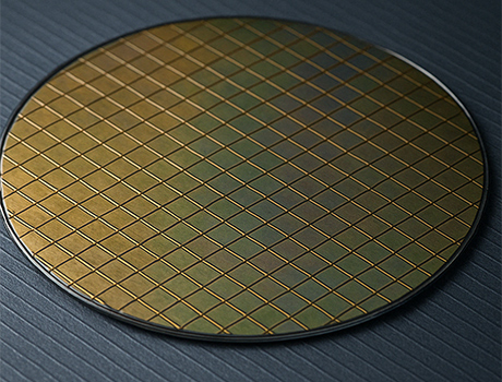
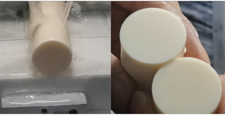
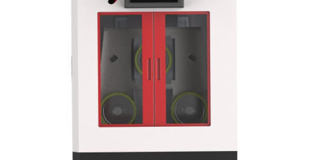
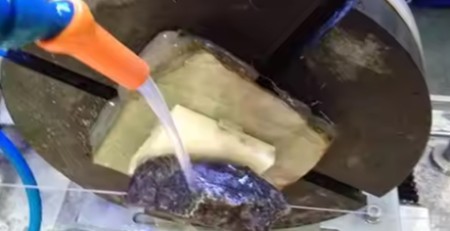
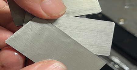
Semiconductor wafer slicing is a critical IC manufacturing step where precision and surface integrity determine device yield.
A diamond cutting wire loop is a closed loop of diamond-coated wire that slices ingots with ultra-precise, minimal kerf loss.
Its key advantages are lower thermal and mechanical stress than laser or blade cutting, which matters most as wafers get thinner.
Semiconductor wafer slicingis a critical process in the manufacturing of integrated circuits (ICの) およびその他のマイクロエレクトロニクスデバイス. 精度と効率は最優先事項です, 小さな欠陥でも、最終製品で重大なパフォーマンスの問題につながる可能性があるためです. 利用可能なさまざまな切断技術の中で, ダイヤモンドカッティングワイヤーループは、その卓越した精度により、優れた方法として浮上しています, 最小限の材料損失, 工具寿命の延長.
この記事の内容, we will explore whyダイヤモンドワイヤー切断is becoming the preferred choice for semiconductor wafer dicing and how it outperforms traditional methods like blade sawing and laser cutting.
The Challenges of Semiconductor Wafer Cutting
Semiconductor wafers, typically made of silicon, are extremely thin and fragile. The cutting process must ensure high precision with minimal kerf width and chipping, low thermal damage to prevent microcracks, and high throughput for cost-effective production.
Traditional methods such as mechanical blade sawing can cause microcracks and material loss, while laser cutting may introduce thermal stress. This is where diamond cutting wire loop technology excels.
What Is Diamond Cutting Wire Loop?
A diamond cutting wire loop is a thin, flexible wire embedded with diamond abrasive particles. It operates by continuously moving the wire across the wafer, enabling precise and smooth cuts with minimal mechanical stress. .
Key Advantages of Diamond Wire Cutting
Ultra-Precise Cutting with Minimal Kerf Loss
Diamond wire cutting produces an extremely narrow kerf, as small as 20-30 µm, allowing for higher wafer yield compared to blade sawing. The fine abrasive action reduces chipping and edge defects, crucial for delicate wafers.
Reduced Material Waste
Since the wire is much thinner than a saw blade, less silicon is wasted, improving material utilization and lowering production costs.
Lower Thermal and Mechanical Stress
Unlike laser cutting, diamond wire cutting generates minimal heat, preventing thermal damage to the wafer. The process applies uniform pressure, reducing the risk of microcracks.
Longer Tool Life and Lower Maintenance
Diamond is one of the hardest materials, ensuring durability and consistent performance over extended use. Unlike blades that wear out quickly, diamond wire maintains sharpness for longer, reducing downtime for replacements.
Versatility in Cutting Various Materials
Besidesシリコンウエハ, diamond wire loops can cut gallium arsenide (GaAsの), サファイア, and ceramic substrates with high precision.
Applications in Semiconductor Manufacturing
Diamond wire cutting is widely used in wafer dicing for separating individual chips from a wafer, thin wafer processing for advanced 3D IC stacking, and solar cell manufacturing for cutting silicon ingots into wafers.
結論
The diamond cutting wire loop method offers unparalleled advantages in semiconductor wafer cutting, including higher precision, reduced waste, lower stress, and longer tool life. As the demand for thinner and more efficient wafers grows, this technology is set to become the industry standard.
Manufacturers looking to improve yield and reduce costs should consider adopting diamond wire cutting for their wafer dicing processes. With continuous advancements in wire technology, 私たちは将来的にさらに高い効率と性能を期待できます.
Key Takeaways
The best magnetic material cutting manufacturers combine diamond wire saw technology, tight tolerances and zero thermal damage — the... 続きを読む