Four Cutting Technologies: A Comparative Overview:
1. ダイヤモンドワイヤーループ切断
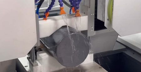
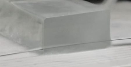
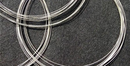
Principle: A fast-moving loop of wire, coated with diamond particles, acts as a cutting tool, grinding through the material. Coolant is often used.
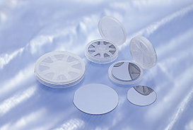
Key Advantage:Low stress, 高精度, minimal material waste. ザ “flexible” wire is gentle on brittle materials, enabling clean cuts with almost no edge chipping. It is the preferred method for slicing high-value, hard, brittle materials like SiC, GaNの, サファイア, そして 光学ガラスinto thin wafers.
Limitation:Limited cutting speed. As a grinding process, its material removal rate is slower than thermal methods like laser cutting, making it less efficient for high-volume or rough cutting jobs.
2. Diamond Saw Blade Cutting
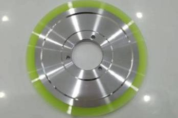
Principle:A rotating circular blade with a diamond-coated edge cuts through the material, similar to a precision stone cutter.
Key Advantage:Proven technology, 高効率, relatively low cost. It’s the standard method for rough cutting and sizing blocks of silicon and ceramic.
Limitation:High mechanical impact. It can easily cause edge chipping and internal stress or micro-cracks, making it unsuitable for finishing ultra-thin, ultra-hard, or high-value materials.
3. レーザー切断
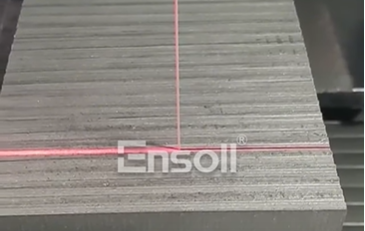
Principle:A focused, high-energy laser beam melts, vaporizes, or alters the material, with a gas jet removing the debris.
Key Advantage:Non-contact, no tool wear, very fast, highly flexible. It easily handles complex 2D shapes and can perform “stealth dicing” (separation via internal modification), making it ideal for wafer dicing and shaping silicon, サファイア, and glass.
Limitation:Creates a heat-affected zone that may change material properties at the cut edge. It can struggle with highly reflective (例えば。, pure copper) or transparent materials. Equipment is expensive.
4. Electrical Discharge Cutting (ワイヤー放電加工)
Principle:Controlled spark discharges between a thin wire electrode and the workpiece generate intense heat, locally melting and vaporizing the material.
Key Advantage:Cuts any conductive material regardless of hardness (例えば。, hardened steel, 炭化タングステン, conductive ceramics). It achieves very high precision and can create complex shapes.
Limitation:Only works on conductive materials. The process is slow, and it leaves a recast layer on the cut surface.
Summary & Selection Guide
There is no single “best” technology—each is most suitable for specific tasks:
For ultimate cut quality and minimal loss when slicing hard, brittle wafers (例えば。, ティッカー): Chooseダイヤモンドワイヤーループ 切断.
For efficient, low-cost rough cutting of hard, brittle blocks: Choose Diamond Saw Blade Cutting.
For high-speed cutting of complex 2D shapes in various materials (including non-metals): Choose Laser Cutting.
For machining intricate shapes in very hard, conductive materials (例えば。, molds): Electrical Discharge Cutting is the only choice.
A semiconductor is a material whose electrical conductivity sits between a conductor and an insulator and can be controlled by doping, making it the foundation of integrated circuits.
What are the main types of semiconductor materials?
Silicon dominates general ICs; compound semiconductors include gallium arsenide (RF, optoelectronics), 窒化ガリウム (high-frequency power) および炭化ケイ素 (high-voltage, high-temperature power).
Where are SiC and GaN semiconductors used?
SiC is used in EV inverters and high-voltage power modules, while GaN is used in fast chargers, RF power amplifiers and 5G infrastructure.
Key Takeaways
Steel guide wheels deliver maximum rigidity and dimensional stability for high-precision diamond wire cutting, but transmit more vibration to... 続きを読む