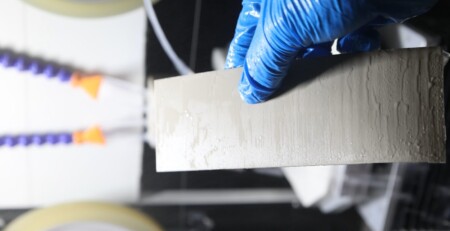
В сложном мире производства полупроводников, путь от необработанного слитка кремния до высокопроизводительной интегральной схемы является чудом современной инженерии. В самом начале этого пути лежит процесс, который определяет эффективность всей цепочки поставок:Резка кремниевых пластин.
Пока мы празднуем 2026 Фестиваль фонарей и с нетерпением ждем года “Лучшего” производство, Ensoll гордится тем, что возглавляет разработку решений для высокоточной резки. Для производителей, the choice of cutting tool is no longer just a procurement decision—it is a strategic move that dictates yield, стоимость, and global competitiveness.
The fullпроцесса резки алмазной проволокой— from ingot mounting to wafer cleaning — is documented step by step in our monocrystalline silicon guide.
1. The Critical Role of Silicon Wafer Cutting
Silicon remains the “bedrock” of the digital age. Whether it is Monocrystalline Silicon for high-efficiency CPUs or Polycrystalline Silicon for solar arrays, the goal of slicing is always the same: to produce thin, flat, and damage-free wafers with the least amount of material loss.
The Challenge of “The Kerf”
В полупроводниковой промышленности, silicon is essentially “liquid gold.” When an ingot is sliced, the thickness of the cutting tool creates a gap called the kerf. The material in this gap is turned into fine dust (стружка) and lost forever. Traditional sawing methods often lose up to 30% Кому 40% of the ingot to kerf loss.
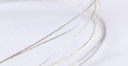
Ensoll’sАлмазная канатная пилаtechnology addresses this head-on. By utilizing ultra-thin wires (as thin as 80μm to 120μm), we minimize the “gap” and maximize the number of wafers harvested from a single ingot.
Видеовитрина: High-Speed Silicon Slicing
2. Why Diamond Wire Saw Outperforms Traditional Methods
For decades, the industry relied on Slurry Wire Saws (using loose silicon carbide grit in a liquid carrier). Однако, as we move into 2026, DWS has become the undisputed champion. Вот почему:
A. Fixed Abrasive Efficiency
In a slurry saw, the grit “rolls” between the wire and the silicon, leading to a chaotic and slow cutting action. In an Ensoll Diamond Wire, the diamonds are electroplated directly onto the wire. This “fixed abrasive” method allows for:
Faster Linear Speeds: Reducing cutting time by up to 75%.
Lower Cutting Force: Minimizing the risk of wafer breakage.
B. Superior Surface Geometry
Semiconductor wafers must be perfectly flat. Any “bow” or “деформация” can cause errors during the subsequent lithography process. Ensoll’s wire saws provide:
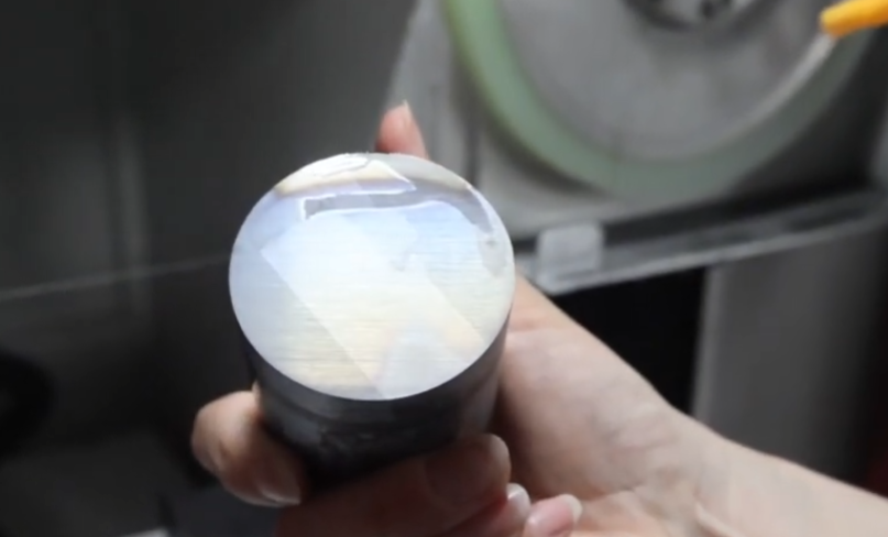
Unmatched TTV (Изменение общей толщины): Ensuring every wafer is uniform from edge to center.
Reduced Saw Marks: A smoother surface means less time spent in the expensive Chemical Mechanical Polishing (CMP) stage.
Image Showcase: Surface Quality Comparison
3. The Technical Heart of Ensoll: Our Diamond Wire Construction.
Not all diamond wires are created equal. В Ensoll, our R&D has perfected a proprietary electroplating process that ensures the longevity and performance of our tools.
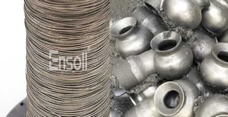
High-Tensile Core: We use premium high-carbon steel that can withstand the extreme tension required for high-speed wafering without snapping.
Diamond Grit Selection: We use synthetic diamonds with specific crystalline shapes to ensure maximum “bite” into the silicon.
Uniform Distribution: Наш “Лучшего” 2026 manufacturing line ensures that diamond particles are distributed with mathematical precision, предотвращая “bald spots” on the wire that cause uneven cuts.
4. Expanding Beyond Silicon: SiC и GaN
The semiconductor landscape is shifting toward Wide Bandgap (WBG) materials like Silicon Carbide (Так). These materials are nearly as hard as diamond itself, making them notoriously difficult to cut.
Ensoll’s diamond wire saw tools are specifically engineered for these “hard and brittle” challenges. By optimizing the bond between the diamond and the wire, we allow for the efficient slicing of SiC ingots, which is crucial for the burgeoning Electric Vehicle (Электромобиль (EV)) and 5G Power industries.
5. Environmental and Economic Impact: The Green Advantage
Sustainability is a core pillar of Ensoll’s 2026 mission. Traditional slurry sawing produces large amounts of toxic waste that is difficult to recycle.
Zero Slurry: DWS uses water-based coolants that are significantly easier to filter and recycle.
Energy Efficiency: Faster cutting times mean lower energy consumption per wafer.
Cost Reduction: By reducing kerf loss and polishing time, Ensoll helps manufacturers lower their Cost Per Wafer significantly.
6. Ensoll’s 2026 Service Guarantee: Our Three Promises
As highlighted in our Lantern Festival commencement, we are not just providing tools; we are providing a “Fullfillment” package:
Precision Fulfillment: We guarantee that our wires will maintain consistent diameters throughout their lifespan, ensuring stable yields.
Service Fulfillment: Our Global 4-hour response team is active in every major tech hub (from Singapore to the UAE) to troubleshoot and optimize your lines.
Partnership Fulfillment: We work with your engineers to customize wire specifications for your specific ingot sizes and machine types.
Silicon wafer cutting is the first cost-defining step in semiconductor fabrication: kerf loss directly sets how many wafers one ingot yields.
Diamond wire saw outperforms ID blades and slurry saws because fixed diamond abrasive gives a narrower kerf, better surface geometry and less material waste.
Ensoll diamond wire combines electroplated diamond grit with high-tensile steel wire, keeping tension stable and wire life long in production slicing.
The same diamond wire platform extends beyond silicon to SiC and GaN substrates with adjusted speed, tension and coolant parameters.
Заключение: Тем “Лучшего” Way to Cut
The semiconductor industry moves at light speed, and your cutting technology must keep pace. Silicon Wafer Cutting is the foundation upon which all modern technology is built. By partnering with Ensoll and utilizing our advanced Diamond Wire Saw solutions, you are choosing a path of higher efficiency, снижению отходов, and superior precision.
As we light the lanterns for 2026, let us light the way for your production line. Experience the “Precision Fulfillment” that only Ensoll can provide.
Часто задаваемые вопросы
Why is diamond wire saw the standard for silicon wafer cutting?
Fixed diamond abrasive cuts with a narrow kerf (обычно 120-250 мкм), holds tight TTV and wastes far less silicon than ID blades or slurry sawing, so more wafers are produced per ingot.
What is kerf loss and why does it matter?
Kerf loss is the width of material removed by the cut. Every micrometer saved means more wafers per ingot, which is the dominant cost lever in silicon wafer production.
Can the same diamond wire saw cut SiC and GaN?
Да. Diamond wire handles hard, brittle materials well; only process parameters such as wire speed, tension and coolant need to be adjusted for each material.
What surface quality does diamond wire cutting achieve?
As-cut surfaces typically reach Ra 0.2-0.5 µm with minimal sub-surface damage, which shortens downstream lapping and polishing time.
Технический контент проверен инженерной командой Ensoll — производителя алмазных проволочных петель с 10+ многолетним производственным опытом.
Карбид кремния (Так), известен своей исключительной твердостью и долговечностью, широко используется в различных отраслях промышленности. Чтобы эффективно сократить это... читать далее
Петля из алмазной проволоки технология резки революционизировала точную резку в производстве полупроводников и обработке материалов. Этот продвинутый метод использует алмазно-пропикантное.... читать далее
Основные выводы
Резка полупроводниковых пластин является критически важным этапом производства интегральных схем, где точность и целостность поверхности определяют выход годных изделий.
Алмазная резка... читать далее
Основные выводы
Алмазные проволочные пилы режут вольфрамовые стержни с использованием проволоки с алмазными частицами - один из немногих практических.... читать далее
В мире промышленной резки, Точность и эффективность имеют первостепенное значение. Одно инновационное решение, которое набирает популярность в последнее время... читать далее
Петля из алмазной проволоки стали предпочтительным решением для резки твердых, хрупких материалов, таких как ферритовые сердечники, магниты Alnico,... читать далее
Абстрактный: В этой статье представлен тест точного нарезки на PEEK (полиэфирном эфирном кетоне) с использованием а Петля из алмазной проволоки. Тем... читать далее