违约

Ensoll工具的综合文章和更新.

碳化硅晶片的应用 & 趋势

Silicon carbide wafer application and future development trend Key Takeaways Silicon carbide is the main development direction of the power semiconductor industry. SiC wafers enable devices that run at higher voltage, frequency and temperature than silicon, cutting energy losses in EVs, fast charging and grid equipment. The industry trend is toward larger SiC wafer diameters and lower defect densities. 碳化硅 (原文如此) 是功率半导体行业的主要发展方向, and its use in the manufacture of power devices can significantly improve power...
如何加工碳化硅?

如何加工碳化硅? Key Takeaways Silicon carbide is the key material of the power semiconductor industry, but its hardness makes every processing step demanding. SiC processing flows from crystal growth through slicing, grinding and polishing, with diamond-based tooling used at each hard-material step. 碳化硅 (原文如此) 材料是功率半导体行业的主要发展方向. 用于制造功率器件,可显著提高电能利用率. 在可预见的未来, new energy vehicles will...

金刚石线环锯切割钕铁硼磁铁

Diamond wire loop saw cutting NdFeB magnet Key Takeaways NdFeB magnets are tetragonal Nd2Fe14B crystals — the strongest commercial permanent magnets in use today and the most common rare-earth magnet across electronics, motors, medical equipment and aerospace. There are two types: bonded NdFeB, which is magnetically isotropic and corrosion-resistant, and sintered NdFeB, which is stronger but corrodes easily and must be plated (zinc, 镍, or nickel-copper-nickel coatings). Traditional cutting routes are reciprocating long-wire saws for large magnets and inner-diameter (ID) slicing machines for small...

传统太阳能电池生产工艺

Traditional solar cell production process Key Takeaways Traditional solar cell production starts with silicon wafer manufacturing and proceeds through texturing, 扩散, 蚀刻, coating and metallization. Wafer slicing quality — kerf, TTV and surface damage — directly affects cell efficiency and yield. Before we always described the manufacturing principle and processing process of silicon wafers, 今天我们就来介绍一下传统太阳能电池的生产工艺. 传统电池生产主要可归纳为 6 步骤. 从传统电池制造工艺的角度来看, it...

硅片在光伏行业的繁荣

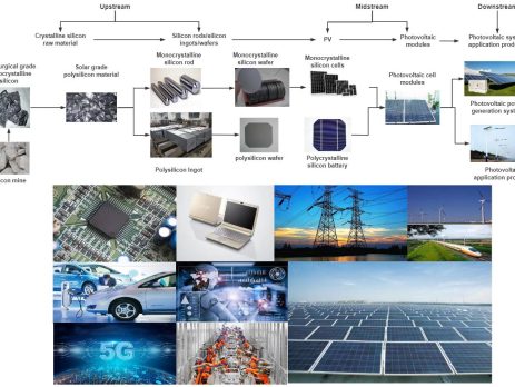
The boom of silicon wafers in the photovoltaic industry Key Takeaways Carbon-neutrality goals worldwide have made photovoltaics the fastest-growing source of demand for silicon wafers. PV wafer economics are driven by kerf loss and throughput, which is the main reason diamond wire replaced slurry saws across the industry. Larger wafer formats and thinner wafers are the PV industry's structural cost-reduction path, and both raise the bar for cutting precision. 碳中和目标和全球清洁能源加速应用背景下,...

2022 半导体晶圆产业概要

2022 Semiconductor Wafer Industry Overview Key Takeaways Semiconductor silicon wafers are the carrier substrate for chip manufacturing, and the wafer industry is highly concentrated and technology-intensive. Industry development is driven by larger wafer diameters, tighter flatness specs and growing demand from logic, memory and power devices. 半导体硅晶圆是制造芯片的载体, 也被称为硅片,因为原材料是硅. 经过规划和管理的免硅精炼, 纯化, 单晶硅生产, 晶圆成型和其他工艺, it can enter the...

金刚线硅片切割设备的趋势

1) High line speed and high production capacity support the reduction of single GW investment According to the theory of fracture mechanics and the properties of silicon materials, 当金刚石磨粒的最大切削深度大于硅材料的临界切削深度时, 将发生从塑性切削到脆性断裂切削的转变. 所以, 在金刚石线负载的允许范围内, appropriately increasing the steel wire speed in the multi-wire cutting process is beneficial...

光伏硅片的尺寸变化

Key Takeaways Photovoltaic silicon wafer sizes evolved from semiconductor wafer formats, with PV historically lagging semiconductors in dimension standards. Wafer dimensions keep growing (from 156 mm to 182/210 mm classes) because larger wafers cut module cost per watt. Larger and thinner wafers raise the precision bar for slicing equipment and diamond wire. 光伏硅片的尺寸来源于半导体硅片. 在发展方面 , 光伏落后于半导体 1 到 2 代. 多年来, the size of...