使用钻石线环精密切割硅棒
抽象: This article presents a comprehensive study on the precision slicing of silicon rods using a 金刚石线环. The test workpiece was a φ330 mm × 500 mm silicon rod sourced from a European customer, sliced into 10 mm-thick wafers on an Ensoll ESC600-4T single-cantilever machine. We report the cutting parameters, cooling strategy, and quantitative quality metrics including Total Thickness Variation (TTV), dimensional tolerance, 表面粗糙度 (Ra), and edge chipping. The results demonstrate that an optimized diamond wire loop process can achieve stable, high-precision silicon slicing suitable for downstream semiconductor and photovoltaic applications.
- A φ330 mm × 500 mm silicon rod was sliced into 10 mm wafers on the Ensoll ESC600-4T diamond wire loop machine (0.50 毫米线, 38 米/秒, 210 N tension).
- Optimizing feed parameters cut TTV from 0.170 mm to 0.070 mm across three test runs.
- Average surface roughness stayed below 1 μm Ra with minimal edge chipping.
1. 介绍
Silicon is the backbone of the modern semiconductor and photovoltaic industries. Monocrystalline silicon wafers demand exceptionally tight tolerances: minimal thickness variation, low surface roughness, and near-zero edge chipping. Achieving these specifications on large-diameter silicon rods is challenging because silicon is both hard and brittle, with relatively low fracture toughness. During abrasive cutting, concentrated thermal and mechanical loads can trigger brittle fracture, propagate subsurface micro-cracks, and produce edge chipping and thickness inconsistency.
To address these challenges, Ensoll Tools designed a dedicated process for high-precision linear slicing of silicon rods. The approach combines continuous water cooling to suppress cutting-zone temperature rise, optimized feed parameters matched to the material, and a custom single-cantilever diamond wire loop cutting machine (ESC600-4T). By aligning machine structure, cooling conditions, and cutting parameters, the process minimizes thermal and mechanical damage to both the wafer surface and edges, delivering the dimensional accuracy, thickness uniformity, and surface quality required for advanced silicon applications.
2. Test Object and Material Properties
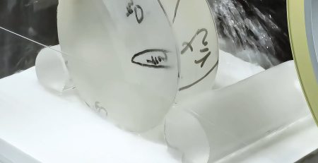
The workpiece for this study was supplied by a European customer (referred to as Customer F). The key material and geometry data are summarized below:
- 材料: Silicon rod
- 硬度: Mohs ~6.0–6.5
- 工件尺寸: φ330 mm × 500 毫米 (L)
- Target slice thickness: 10 毫米
Silicon’s combination of high hardness and brittleness makes it a classic representative of hard-and-brittle materials. Any cutting technology applied to silicon must simultaneously control abrasive wear, heat accumulation, and brittle-mode material removal.
The same hard-and-brittle behaviour sets the practical feed limit when 切割氧化铝陶瓷, where chipping rather than tool wear is the binding constraint.
3. 机器及线材选择
The cutting trials were performed on an Ensoll ESC600-4T single-cantilever diamond wire loop cutting machine. This model was developed specifically for large-diameter silicon-rod slicing, taking into account the material’s hardness, 脆性, and the geometric tolerances demanded by semiconductor-grade processing.
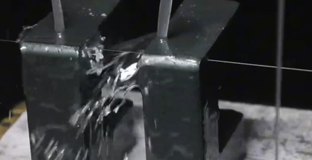
- 冷却液: Water. Water offers high specific heat capacity and excellent convective heat transfer, making it ideal for reducing cutting-zone temperature and flushing away silicon debris. Continuous water supply improves interface cleanliness, cutting stability, and final surface quality.
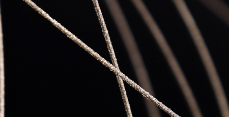
- 线材类型: Fully electroplated diamond wire loop. The electroplated bond ensures high-density, uniform diamond-grain distribution and strong grain retention. This configuration maximizes effective cutting edges, improves wire durability, and reduces surface damage and edge chipping.

4. 切割方法及机器优势
The ESC600-4T integrates several structural and control features that directly benefit silicon-rod slicing:
- Gantry cutting architecture: A high-rigidity gantry frame drives the cutting assembly vertically. This layout maintains structural stability and motion accuracy throughout the cut, suppressing vibration and trajectory deviation. The result is improved perpendicularity and dimensional consistency across each slice.
- Moving-head, 固定工件设计: 切割组件移动,而硅棒保持静止. 消除工件运动可保持加工基准,并在相同锭尺寸下允许更紧凑的机器占地.
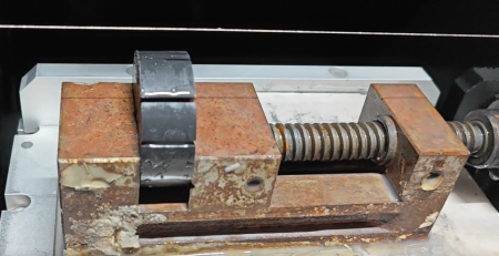
- 可调V型支撑平台: 可调节的V型支撑结构可以重新定位以匹配棒材直径, 确保夹持稳定,并适应各种硅棒规格.
- 液压装载台: 液压升降装置负责棒材的装载和定位, 在手动操作过程中减少冲击和位置漂移. 切割时升降装置也会收回支撑结构范围之外, 防止干扰.
- 智能张力控制: 张紧系统根据运行状态和线径磨损持续调整丝绳张力, 保持金刚石线圈在稳定的张力范围内. 空闲时, the system relaxes tension to minimize long-term load on both the wire and guide-wheel grooves; upon restart, working tension is restored rapidly.
5. 切割参数与冷却
The principal cutting parameters were selected based on the silicon material properties, 这 10 mm target slice thickness, and preliminary process verification. The parameter set is summarized in Table 1.
| 参数 | 数值 |
|---|---|
| 线径 (毫米) | 0.50 × 3,570 |
| 进给速度 (毫米/分钟) | 15 / 18 / 25 |
| 切割宽度 (毫米) | 330 |
| 导丝张力 (N) | 210 |
| 导丝速度 (米/秒) | 38 |
| Wire bow time (秒) | 200 |
Water was supplied continuously as the coolant throughout all cuts. Three feed speeds were evaluated—15, 18, 和 25 mm/min—to investigate the influence of removal rate on slice quality.

6. 切割结果
Three slices (labeled S01, S02, and S03) were produced and subjected to metrological inspection. Each sample was measured for Total Thickness Variation (TTV), dimensional tolerance, 表面粗糙度 (Ra), and edge chipping.

6.1 总厚度变化 (TTV)
TTV was measured using a vacuum-chuck nine-point grid dual-probe thickness gauge. The equipment was thermally equilibrated and calibrated with certified thickness blocks before testing. Samples were cleaned in a dust-free environment, centered on the vacuum chuck, and held flat by negative pressure to minimize warpage-induced error.
| 样品 | Nine-point thickness (毫米) | T最大值 (毫米) | T最小值 (毫米) | TTV (毫米) |
|---|---|---|---|---|
| S01 | 9.780, 9.750, 9.760, 9.820, 9.650, 9.720, 9.790, 9.730, 9.770 | 9.820 | 9.650 | 0.170 |
| S02 | 9.926, 9.977, 9.952, 9.961, 9.936, 9.885, 9.948, 9.920, 9.950 | 9.977 | 9.885 | 0.092 |
| S03 | 10.006, 10.071, 10.075, 10.073, 10.005, 10.066, 10.032, 10.048, 10.058 | 10.075 | 10.005 | 0.070 |
Evaluation: The nine-point TTV data show that S03 delivered the best thickness uniformity (0.070 毫米), while S01 exhibited the largest variation (0.170 毫米). As feed speed increased from 15 mm/min to 25 毫米/分钟, TTV 单调改善, 表明适度提高进给速度在结合适当的冷却和张力控制时,可以稳定切削过程并减少厚度波动.
6.2 Thickness Dimensional Tolerance
厚度公差相对于标称厚度进行评估 10.000 mm,使用相同的九点网格数据. 每个测量点计算正偏差和负偏差,并在三片切片中进行汇总.
| 样品 | Average thickness (毫米) | 厚度偏差 (毫米) |
|---|---|---|
| S01 | 9.641 | −0.359 |
| S02 | 9.939 | −0.061 |
| S03 | 10.048 | +0.048 |
| 最大正偏差 | +0.048 | — |
| 最大负偏差 | −0.359 | — |
| 整体厚度公差 | ±0.359 | — |
Evaluation: 厚度偏差主要为负值. S01 显示出明显的偏薄现象 (−0.359 mm), 这拓宽了整体公差带. S02 和 S03 逐渐接近标称尺寸, indicating improved dimensional control stability at higher feed speeds. The trend confirms that feed-rate optimization is a critical lever for thickness accuracy in 硅片切割.
6.3 表面粗糙度 (Ra)
Surface roughness was measured with a stylus profilometer according to ISO 4287. The measurement direction was aligned with the dominant surface texture orientation. Three locations were inspected on each slice: center, left-mid, and right-mid.
| 样品 | Ra-1 (微米) | Ra-2 (微米) | Ra-3 (微米) | 平均Ra (微米) |
|---|---|---|---|---|
| S01 | 0.860 | 0.640 | 0.690 | 0.730 |
| S02 | 0.910 | 0.960 | 0.680 | 0.850 |
| S03 | 0.760 | 0.670 | 0.800 | 0.743 |
Evaluation: Average Ra values ranged from 0.730 μm to 0.850 微米, with an overall spread of 0.640–0.960 μm. The small variation between measurement positions on each slice indicates a uniform surface texture, confirming that the diamond wire loop run and material removal remained stable throughout the cut. These Ra levels are consistent with high-quality abrasive slicing of silicon and compare favorably with results reported in our precision slicing of metal tubes case study.
6.4 边缘碎裂
Edge chipping was quantified by optical microscopy on all four edges of each slice. Samples were cleaned, the microscope scale was calibrated, and all four sides were scanned sequentially.
| 样品 | 位置 1 (微米) | 位置 2 (微米) | 位置 3 (微米) | 位置 4 (微米) | 最大崩缺 (微米) |
|---|---|---|---|---|---|
| S01 | 5.6 | 7.2 | 6.4 | 8.1 | 8.1 |
| S02 | 6.3 | 8.5 | 7.1 | 9.2 | 9.2 |
| S03 | 5.1 | 6.8 | 7.4 | 8.6 | 8.6 |
Evaluation: Chipping sizes ranged from 5.1 μm to 9.2 微米, with mean maximum chipping of 8.6 微米. The relatively narrow distribution across all samples indicates stable material removal at the kerf boundary. Edge integrity at this level is acceptable for many semiconductor preprocessing steps and can be further improved with parameter refinement.

7. 结论
The silicon-rod slicing trials demonstrate that a well-matched combination of machine architecture, coolant system, and cutting parameters can deliver high-precision results on large-diameter silicon billets. The key findings are:
Shops specifying equipment for large-diameter work can compare gantry and cantilever architectures in our overview of the 金刚石绳锯切割机.
- Machine structure matters. The single-cantilever ESC600-4T gantry design provides the motion stability and clamping adaptability needed for φ330 mm silicon rods. By isolating machine vibration from the wire trajectory, the cantilever layout establishes a solid foundation for thickness control and cutting consistency.
- Cooling is non-negotiable. Continuous water cooling effectively suppresses cutting-zone temperature rise, flushes abrasive debris, and maintains a clean wire–workpiece interface. The reduction in thermal load and particulate contamination directly translates to more stable cutting and better surface integrity.
- Feed-rate optimization pays off. Raising the feed speed from 15 mm/min to 25 mm/min progressively reduced TTV from 0.170 mm to 0.070 毫米. This confirms that, within the tested window, a faster feed can stabilize the material-removal process and improve thickness uniformity when paired with adequate cooling and tension control.
Collectively, the TTV, thickness tolerance, 表面粗糙度 (Ra), and chipping data validate that the optimized 金刚石线环 process on the ESC600-4T is capable of producing silicon slices that meet the stringent requirements of photovoltaic and semiconductor downstream processing. The results provide a practical process baseline for engineering-scale silicon-rod slicing and can be adapted to other hard-and-brittle materials of comparable hardness and geometry.
有关Ensoll硅材料金刚石线环解决方案的更多信息, 磁性材料, 陶瓷, 和金属, 请查看我们的 精密切割指南 或联系工程团队.
这些结果与我们在更广泛研究中的工作相关 silicon wafer slicing, 相同参数用于更薄晶圆的调节.常见问题
金刚石线环切割硅棒时可以达到的总厚度变异(TTV)是多少?
在这次针对φ330毫米硅棒进行的ESC600-4T测试中, total thickness variation (TTV) 通过在三次运行中优化进给参数,从而改善到 0.170 mm to 0.070 毫米.
金刚石线环切割硅表面粗糙度是多少?
该研究中样本的平均Ra保持在 1 微米以下——足够光滑,可在许多应用中减少或消除后续研磨.
用于此次硅棒切割研究的机器是哪一款?
Ensoll ESC600-4T单悬臂金刚石线环切割机, 运行于 0.50 mm diamond wire loop at 38 m/s wire speed and 210 N tension.
Why use a diamond wire loop instead of a slurry saw for silicon rods?
The loop cuts with fixed diamond abrasive in a water-cooled, single-direction pass, giving a narrower kerf, less sub-surface damage, and shorter cycle times than loose-abrasive slurry sawing.
技术内容由Ensoll工程团队审核——一家金刚线环制造商 10+ 多年生产经验.