切割SiC/GaN: 钻石线锯如何解决这一问题

切割SiC/GaN: 钻石线锯如何解决这一问题

关键要点

  • SiC and GaN are third-generation semiconductors transforming power electronics, 5G and EVs — but they are extremely hard to cut.
  • Their ultra-high hardness, brittleness and thermal-stress sensitivity defeat most conventional cutting methods.
  • Diamond wire saw solves SiC/GaN cutting with the hardest abrasive in a cold, low-force, narrow-kerf process.

介绍

的崛起 第三代半导体材料 (碳化硅和氮化镓) 改变了电力电子, 5G, 和电动汽车行业. 然而, 它们极度的硬度和脆性使 精密切割 一个主要的制造业障碍. 本文探讨了 SiC/GaN 晶圆的切割挑战 以及为什么 金刚石线锯 科技 是最优解.

为什么 SiC/GaN 切割很困难?

semiconductor691. 超高材料硬度

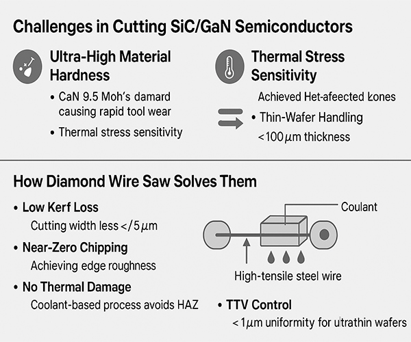
  • 原文如此 (碳化硅): 9.5 莫氏硬度 (靠近 Diamond), 导致工具快速磨损.
  • 赣语 (氮化镓): 高断裂韧性, 容易出现微裂纹.

2. 脆性 & 边缘碎裂

传统切割方法 (例如, 刀片切割) 生成 边缘缺陷 (>20μm 碎裂), 降低产量 功率器件射频芯片.

3. 热应力敏感度

激光切割诱导 热影响区 (HAZ 系列), 改变对高频应用至关重要的材料特性.

4. 薄晶圆处理

用于先进封装的 SiC/GaN 晶圆 (例如, 小芯片设计) 需要 <100μm 厚度 具有亚 1μm TTV (总厚度变化).

金刚石线切割: 最佳解决方案

1. 金刚石绳锯的工作原理

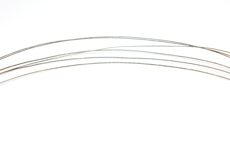
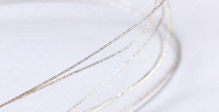
  • 电镀金刚石颗粒(5–50微米) 在高强度钢丝上.

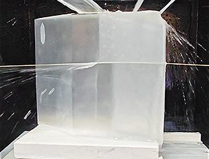
无尽金刚石线锯 9l 往复运动或连续运动 带冷却剂可最大限度地减少热应力.

2. SiC/GaN 的主要优势

  • 低割缝损失: <50μm 切割宽度 VS. 200刀片切割中的 μm (节省材料).
  • 接近零的碎屑: 达到 <5μm 边缘粗糙度 (critical 用于 HEMT 设备).
  • 无热损伤: 基于冷却剂的工艺避免了 HAZ.
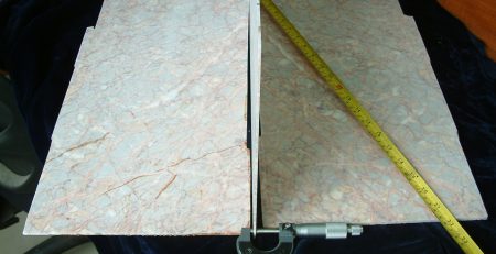
  • TTV 控制: <1μm 均匀性 超薄晶圆.

个案研究: SiC 功率模块生产

半导体一家领先的电动汽车制造商从激光转向 金刚石线切割 用于 SiC MOSFET:

  • 结果 1: 产量从 78% 自 93%(减少裂纹引起的失效).
  • 结果 2: 已达到切割速度 500毫米/分钟使用 0.3μm 金刚石丝

选择合适的金刚石绳锯

用于 SiC/GaN 应用, 优先:

  • 线径: 0.1–0.3 毫米用于精细处理.
  • 金刚石粒度: 10–20μm 用于速度和表面质量之间的平衡.
  • 机器稳定性: 振动 <0.1μm 以防止微裂纹.

未来趋势

  • 混合切割: 将金刚石线与激光预切槽相结合,用于 异构集成.
  • 基于 AI 的过程控制: 实时调整 无缺陷切割.

结论

金刚石绳锯技术解决了 硬度, 脆性, 和热挑战 SiC/GaN 切割, 实现更高的产量和更薄的晶圆. 对于半导体制造商, 投资 精密金刚石线设备 对于扩展下一代设备至关重要.

寻找 SiC/GaN 切割解决方案? 联系我们 免费咨询根据您的需求量身定制的 Diamond 绳锯系统.
For a full process walkthrough, see how to process silicon carbide from slicing through to finish.

常见问题

Why are SiC and GaN so difficult to cut?

Both materials combine Mohs 9-class hardness with brittleness and sensitivity to thermal stress, so blades wear fast and lasers risk heat-induced cracks.

How does diamond wire saw solve SiC and GaN cutting?

Diamond abrasive handles the hardness, while the cold, low-force wire process avoids thermal damage and minimizes edge chipping and sub-surface cracks.

What is third-generation semiconductor material?

Wide-bandgap semiconductors such as SiC and GaN that operate at higher voltage, frequency and temperature than silicon, driving power electronics, 5G and EV applications.

技术内容由Ensoll工程团队审核——一家金刚线环制造商 10+ 多年生产经验.