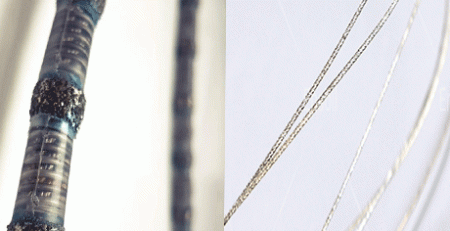
用于光伏的无限金刚石线环 & 半导体
全球向清洁能源和先进计算的过渡给光伏 (光伏) 太阳能和半导体行业的供应链带来了前所未有的压力. 这两个行业的核心都是一个单一, foundational material: high-purity silicon. Whether it is monocrystalline silicon grown for high-efficiency solar cells or ultra-pure silicon ingots destined for microchips, these crystals must be sliced into incredibly thin, flawless wafers before they can be processed into functional devices.
然而, silicon is notoriously brittle and expensive to grow. As solar panels demand thinner wafers to reduce costs and semiconductor nodes shrink to handle higher frequencies, traditional slicing methods are reaching their physical limits.
To overcome these boundaries, leading manufacturers are shifting away from legacy tools and embracing Endless Diamond Wire Loop 科技. This high-speed precision cutting method is rewriting the rules of material yield, 表面质量, and throughput in wafer manufacturing.
Once the ingot is grown, 硅片切割 decides how much of that expensive crystal ends up as saleable wafers.
The High-Stakes Challenge of Silicon Wafering
Slicing silicon ingots into wafers is one of the most critical and cost-sensitive steps in the entire production line. Because silicon has zero plasticity, forcing a blade or a slow tool through it creates immense localized stress.
When using legacy cutting methods—such as inner-diameter (ID) saws or traditional slurry-based reciprocating wire saws—manufacturers face three major roadblocks:
1. Excessive Material Waste (切缝损失)
Silicon ingots require an immense amount of energy and time to grow in crystallization furnaces. Traditional thick blades or loose abrasive slurry wires create a wide cutting path (kerf). This path turns up to 30% 自 40% of the precious silicon ingot into useless, non-recyclable silicon sawdust (切屑) and slurry. In high-volume PV manufacturing, minimizing this waste is the single fastest way to lower the cost-per-watt of solar modules.
2. 内部损伤 (固态硬盘) and Micro-Cracks
The mechanical shock and heavy feeding force of traditional saws telegraph micro-fractures deep into the interior of the silicon wafer. This sub-surface damage compromises the mechanical strength of the wafer. During subsequent automated handling or chemical etching phases, these micro-cracked wafers easily warp or shatter, severely degrading the factory’s total yield.
3. Strict Geometric Tolerances
Modern photovoltaic cells (especially N-type TOPCon and Heterojunction technologies) and semiconductor devices require wafers with absolute flatness, uniform thickness, and near-zero Total Thickness Variation (TTV). 不断减速并反向的往复锯会导致线振动, 这会在晶圆表面留下波纹和锯痕, 需要大量二次抛光.
解决方案: 无限金刚线环技术
为了解决这些复合问题, 光伏和半导体行业正在采用无限金刚线环.
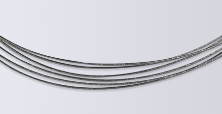
无限金刚线环由高强度, 柔韧钢丝芯组成,并焊接成连续的, 无缝环. 其外表面永久电镀有精确分级的微米级工业金刚石颗粒. 环不是往复移动, 而是在专用高速滑轮系统上连续, 沿单一、连续方向运行.
这种单向, high-speed configuration delivers a massive technological leap forward due to three distinct physical advantages:
Ultra-High Linear Speeds and Gentle Micro-Grinding
While traditional open-loop wire saws travel at relatively low speeds, an endless diamond wire loop can rotate at staggering linear velocities—often between $30\text{ 米/秒}$ and $60\text{ 米/秒}$.
This immense speed completely alters the mechanics of the cut. Because the wire moves so fast, the contact time between any single diamond crystal and the silicon matrix is incredibly brief, dropping the feeding pressure to near zero. The process transitions from a brutal mechanical “锯切” force into a gentle, continuous micro-grinding action. This eliminates the mechanical shock factors that cause micro-fractures, allowing for sharp, chip-free wafer edges.
Ultra-Thin Wires for Maximum Wafer Yield
Because the endless loop maintains perfect, steady tension without the violent “vibration jerk
” associated with reversing directions, the core steel wire can be made exceptionally thin. Today’s industrial loops feature wire diameters down to $0.20\text{ 毫米}$ or less.
The Strategic Benefit: A narrower cutting wire means a narrower kerf. By reducing material waste on every single slice, manufacturers can extract significantly more usable wafers out of a single silicon ingot, maximizing raw material utilization and instantly driving down production costs.
Pristine Surface Quality and Minimal Post-Processing
闭环系统的连续, smooth motion of a closed-loop system entirely eliminates the prominent “往复刀片典型的锯痕” and deep surface gouges typical of slower cutting methods. 由此产生的表面粗糙度 ($R_a$) and Total Thickness Variation (TTV) are remarkably low.
For the photovoltaic sector, 这种干净的 “原切” surface means wafers can go directly into texturing and doping phases. For the semiconductor sector, it slashes the time and labor required for downstream Chemical Mechanical Planarization (CMP) and fine polishing stages.
光伏 & Semiconductor Wafer Slicing Comparison
| Performance Parameter | Traditional Slurry / ID Saws | Endless Diamond Wire Loop |
| Cutting Action | Low-speed mechanical shearing | High-speed, low-force micro-grinding |
| Wire/Blade Thickness | Thick ($0.5\文本{ 毫米}$ – $1.2\文本{ 毫米}$) | Ultra-thin ($0.18\文本{ 毫米}$ – $0.30\文本{ 毫米}$) |
| Material Yield (切缝损失) | 差 (High volume of silicon waste) | 优秀 (Maximum wafers per ingot) |
| 表面光洁度 (TTV / $R_a$) | High variation, prominent saw marks | Extremely flat, near pre-polished surface |
| 内部损伤 (固态硬盘) | Deep micro-cracking risk | Negligible, preserving wafer structural integrity |
For a full parameter walk-through of diamond wire loop slicing of silicon rods (φ330 mm, 10 mm slices), see our engineering case study.
- Photovoltaic and semiconductor wafering share one bottleneck: slicing hard, brittle silicon with minimal kerf loss and sub-surface damage.
- Endless diamond wire loops cut at ultra-high linear speeds with a gentle micro-grinding action that limits micro-cracks and sub-surface damage.
- Ultra-thin diamond wires maximize wafer yield per ingot — the single biggest cost lever in both the PV and semiconductor industries.
结论: Driving Next-Generation Clean Energy and Computing
As the green energy transition accelerates and semiconductor nodes shrink further, manufacturing efficiency must evolve. Wasting premium, energy-intensive crystalline silicon is no longer acceptable in a competitive global market.
The Endless Diamond Wire Loop has proven to be the definitive technological answer for slicing silicon in the photovoltaic and semiconductor fields. By conquering material brittleness, optimizing raw material yields, and delivering flawless surface geometry, this advanced cutting technology stands as a crucial pillar supporting the future of clean solar energy and high-performance computing worldwide.
常见问题
What is an endless diamond wire loop?
It is a closed loop of high-tensile steel wire coated with diamond abrasive, running continuously at high speed to slice hard, brittle materials such as silicon, SiC and sapphire.
Why is kerf loss so critical in wafering?
Every micrometer of kerf is silicon turned into dust. Thinner wire and a narrower cut mean more wafers per ingot, which directly lowers the cost of each wafer.
What is sub-surface damage (固态硬盘)?
SSD is the layer of micro-cracks left beneath the cut surface that must be removed by lapping or etching. The gentle micro-grinding of diamond wire keeps this layer shallow, saving downstream process time.
Can one wire loop platform serve both PV and semiconductor wafering?
是的. The slicing principle is the same; wire diameter, 速度, tension and coolant are tuned to the wafer size and thickness specifications of each industry.
技术内容由Ensoll工程团队审核——一家金刚线环制造商 10+ 多年生产经验.