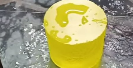
硅晶圆切片——也称为硅晶圆锯切或简称晶圆切割工艺——是将生长的单晶锭制成用于芯片和太阳能电池的薄片的生产步骤. If you are asking how silicon wafers are cut, the short answer is a diamond wire loop running at 10–25 m/s, where wafer thickness and total thickness variation (TTV) are set by wire tension and feed rate. The same physics governs cutting silicon wafers for photovoltaics and for semiconductor substrates; only the thickness target and the tolerance for subsurface damage differ.
But the wafer saw process isn’t a single method. It includes techniques like 金刚石线环 切削, EDM wire cutting, and even compact table top cutter machines for R&D and small-batch production.
关键要点
A diamond wire loop cuts silicon with a 100–300 µm steel wire electroplated or resin-bonded with diamond grit, running at 10–25 m/s under continuous coolant.
Diamond wire replaced ID blades and slurry sawing mainly because of kerf loss — a narrower cut means more wafers per ingot, which is the dominant cost lever in silicon.
The three defect modes to control are wire breakage and wear, surface micro-cracks, and wire bow caused by uneven tension.
Silicon wafer slicing, silicon wafer sawing and the wafer cutting process all describe the same production step: cutting silicon wafers from a monocrystalline ingot with a diamond wire. Production targets are typically 120–250 µm kerf loss with TTV held under 10 微米.
– EDM wire cutting as an alternative for conductive materials
– Table top cutter machines for laboratory and prototyping use
让我们深入探讨:
1. What is a Wafer?
Before discussing how wafers are cut, we need to understand what a wafer actually is.
A wafer is a thin, flat disc of semiconductor material — most commonly silicon — on which microelectronic devices are built. Wafers serve as the substrate for integrated circuits (集成电路), 太阳能电池, LEDs, and MEMS (microelectromechanical systems).
Typical Wafer Sizes
Wafers have grown in diameter over decades:
– 1 inch to 2 英寸 (early 1960s)
– 4 英寸 (100毫米), 6 英寸 (150毫米), 8 英寸 (200毫米)
– 12 英寸 (300毫米) – industry standard today
– 18 英寸 (450毫米) – emerging but rare
Thickness is typically between 500–800 microns, but after polishing and backgrinding, finished IC wafers can be as thin as 50–100 microns.
Why Precision Cutting Matters
A single wafer can yield thousands of individual chips (dies). If the cutting process (dicing) is inaccurate, you lose chips, reduce yield, and increase costs. That’s why the wafer saw process must be extremely precise — often within ±1–5 microns.
2. Wafer Saw Process (金刚石线环)
Now let’s focus on the core of our topic: the wafer saw process using a金刚石线环.
Traditional vs. Diamond Wire Sawing
Historically, wafers were cut from ingots using inner-diameter (ID) blades — circular saws with diamond-impregnated rims. But ID blades have limitations:
– Wide kerf (material loss)
– Slow cutting speed
– Surface damage
Enter diamond wire sawing.
How Diamond Wire Loop Works
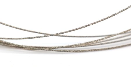
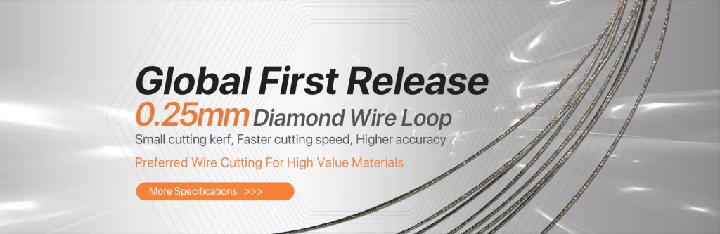
A diamond wire loop consists of a thin steel wire (typically 100–300 microns in diameter) electroplated or resin-bonded with diamond grit. The wire is formed into a continuous loop and driven by pulleys at high speed (10–25 m/s).
随着电线的移动, the diamond grit grinds through the material via a three-body abrasion mechanism. 冷却液 (usually deionized water or oil-based fluid) removes debris and heat.
Key Advantages of Diamond Wire Loop for Wafer Sawing
Criterion
金刚石线环
电火花线切割
Table Top Cutter (金刚石线)
Material type
Non-conductive & hard
Conductive only
Same as diamond wire loop
Typical kerf
120–250 µm
50–150 µm
150–300 微米
表面光洁度
良好 (Ra 0.2–0.5 µm)
优秀 (Ra 0.05–0.2 µm)
良好 (Ra 0.3–0.6 µm)
切割速度
快速 (2–10 毫米/分钟)
慢速 (0.5–3 毫米/分钟)
中速 (1–5 毫米/分钟)
设备成本
高 (工业型) / 中 (台式)
中高
低到中
最佳用于
硅片, 陶瓷, 蓝宝石
模具钢, 硬质合金, 钛
R&D, 小型锭, 易碎材料
逐步晶圆锯工艺 (从锭到晶圆)
1.锭生长 – 通过柴克拉尔斯基法或区熔法生长单晶硅锭.
磨削 – 将硅锭研磨至精确直径.
线锯切割 – 用金刚石线环将锭切成单个晶圆.
边缘倒角 – 晶圆边缘倒角以防崩裂.
研磨 – 去除锯痕并使晶圆平整.
蚀刻 – 去除受损表层.
抛光 – 形成用于光刻的镜面表面.
硅之外的应用
Diamond wire loop sawing isn’t only for硅片. It’s also used for:
– 碳化硅 (原文如此) – wide-bandgap semiconductor
– Gallium arsenide (砷化镓) – RF and LED applications
– Sapphire – for LED substrates and watch crystals
– Ceramic substrates – alumina, 氧化锆
– Quartz and glass – optical and MEMS wafers
3. 电火花线切割 (A Complementary Technology)
While diamond wire sawing is excellent for non-conductive and hard materials, EDM wire cutting (电火花加工) offers a completely different mechanism.
What is EDM Wire Cutting?
EDM wire cutting uses a thin, electrically charged brass or copper wire to erode conductive materials through a series of rapid electrical sparks. The wire never touches the workpiece — instead, sparks jump across a small gap, melting and vaporizing tiny particles.
How It Works
Wire electrode (0.05–3 mm diameter) is continuously fed from a spool.
Deionized water acts as a dielectric fluid, flushing away debris and controlling sparks.
CNC controls move the workpiece relative to the wire.
Sparks occur thousands of times per second, gradually cutting through metal.
When to Use EDM Wire Cutting vs. Diamond Wire Sawing
材料类型
Recommended Method
硅, 陶瓷, 玻璃, 蓝宝石
金刚石线环
Steel, 硬质合金, 钛, Inconel
EDM wire cutting
磁性材料 (钕铁硼, 钐钴)
Both possible; EDM avoids mechanical stress
PCD (polycrystalline diamond)
电火花 加工 (diamond is conductive if doped)
Advantages of EDM Wire Cutting
No mechanical contact → no stress or burrs
Cuts extremely hard metals (HRC 60+)
高精度 (±1–2 microns)
Can cut complex 2D shapes (not just straight slices)
While EDM is rarely used to slice silicon ingots (silicon is only semi-conductive and EDM works poorly on high-resistivity Si), it is used for:
Cutting metalized ceramic substrates
Dicing copper-clad laminates
Slicing tungsten, molybdenum, or Kovar parts used in semiconductor
4. Table Top Cutter Machine
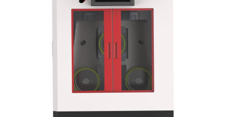
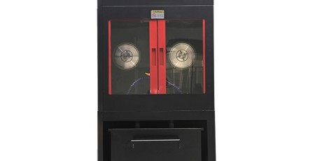
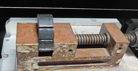
Not every wafer or material cutting job requires a massive industrial saw. For R&D labs, universities, small foundries, and prototype shops, a table top cutter machine is the perfect solution.
Typical Features
Compact footprint (fits on a lab bench)
Adjustable cutting speed and feed rate
Small cutting capacity (typically up to 50–100 mm diameter ingots or blocks)
Integrated coolant system (recirculating or gravity-fed)
Digital readout or CNC control (on high-end models)
混合切割方法: 结合激光预划线 + diamond wire saw for ultra-thin wafers.
结论
The wafer saw process is a cornerstone of modern electronics manufacturing. From growing For conductive materials, EDM wire cutting offers a complementary non-contact method capable of slicing hardened steels, carbides, and superalloys with micron-level accuracy.
And for those working in R&D, prototyping, or small-scale production, a table top cutter machine provides an affordable, flexible entry point into high-precision cutting — without the floor space or budget of an industrial wire saw.
Whether you’re manufacturing 300mm silicon wafers for AI processors or cutting a small alumina substrate on a lab bench, understanding the strengths and limitations of diamond wire loop, 电火花 加工, and table top cutters will help you select the right tool for the job.a silicon ingot to slicing it into hundreds of thin wafers using a diamond wire loop, every step demands precision, cleanliness, and reliability.
常见问题
硅片是如何从锭中切割下来的?
The ingot is grown by the Czochralski or Float Zone method, ground to a precise diameter, then sliced by a diamond wire loop. After sawing, wafer edges are chamfered to prevent chipping, and the wafers are lapped and polished.
硅片切割中的TTV是什么?
TTV (total thickness variation) is the difference between the thickest and thinnest points on a wafer. It is the headline metric for wafer sawing quality because downstream lithography needs a flat, uniform surface.
为什么金刚线取代了浆料切割?
Fixed-diamond wire gives a narrower kerf, a cleaner process with no loose abrasive to manage, and more wafers per ingot. Slurry sawing wastes more silicon per cut and carries higher consumable and disposal costs.
切割更薄的晶片时什么控制断裂?
Real-time tension monitoring, correctly sized diamond grit, and clean filtered coolant. As wafers drop below 150 微米, tension stability and feed control matter more than cutting speed.
What is the difference between diamond wire sawing and EDM wire cutting for wafers?
Diamond wire cuts non-conductive and hard materials with a 120–250 µm kerf at 2–10 mm/min and Ra 0.2–0.5 µm. EDM wire cutting only works on conductive materials, is slower at 0.5–3 mm/min, but produces a finer finish of Ra 0.05–0.2 µm.
What wire diameter is used for silicon wafer cutting?
Typically 100–300 µm steel core wire, carrying diamond grit in the 30–100 µm range, applied by electroplating or resin bonding. Thinner wire reduces kerf loss but needs tighter tension control.
How thin can silicon wafers be cut?
Production solar wafers are commonly 160–180 µm, next-generation cells are moving below 150 微米, and sub-100 µm wafers are the current development target. Each step down demands finer wire and tighter process control.
What causes wire bow, and how is it corrected?
Wire bow is a wavy cut caused by uneven wire tension across the cut. It is corrected with advanced wire guidance systems that apply dynamic tension control throughout the cut.

 Typical Wafer Sizes
 What is EDM Wire Cutting?
 单晶硅是一种高纯度的硅形式,具有单个, 连续晶格结构. 它是使用 Czochralski 生产的 (赵长) 方法或 Float Zone (FZ) 方法, 产生圆柱形铸锭.