単結晶シリコンインゴットの加工フロー
- A single-crystal silicon ingot goes through cropping, diameter grinding, スライス, edge chamfering, lapping and polishing before it is ready for lithography.
- Surface accuracy at the slicing stage determines how much downstream planarization work is required.
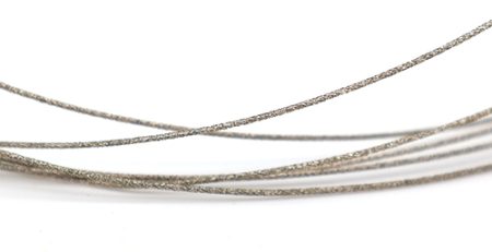
- Diamond wire slicing is the standard way to turn an ingot into bare wafers with tight thickness variation and low sub-surface damage.
単結晶シリコンウェーハ準備段階, the silicon single-crystal ingots need to be processed into raw silicon wafers or barewa-fers with high surface accuracy and surface quality to prepare for planarization for lithography and other processes in the first half of the IC process. ここでは、超平滑で損傷のない基板表面が必要です.
直径≤200mmのシリコンウェーハ用, 従来のシリコンウェーハ処理プロセスは、:
単結晶成長→トリミング→外径バレル研削→フラットエッジまたはV溝処理→ウェーハ→面取り→研削→エッチング→研磨→洗浄→包装 .

外径研削: Since the outer diameter surface of the single crystal silicon rod is not flat and the diameter is larger than the specified diameter specification of the final polished wafer, 外径圧延により、より正確な径を得ることができます.
フラットエッジまたはV溝加工: 参照平面に処理するように指定されています, and the flat edge or V-groove with a specific crystallographic direction on the 単結晶シリコン holder.
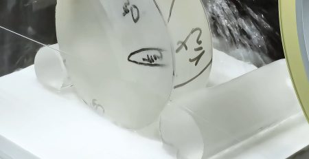
ウエハー: 単結晶シリコンロッドを正確な幾何学的寸法の薄切りに切断することを指します.
面取り: 切断されたウェーハの鋭利なエッジを円弧状にトリミングして、チップエッジの割れや品質不良を防ぐことを指します
研削: 研削によるスライスや砥石研削による鋸痕や表面損傷層の除去を指します, 反りを効果的に変更, 単一製品シリコンウェーハの平坦度と平行度, 研磨工程で対応可能な仕様に到達.
よくある質問
What are the main steps in single-crystal silicon ingot processing?
The typical flow is cropping to length, grinding to precise diameter, slicing into wafers, edge chamfering, then lapping, etching and polishing to reach the surface quality lithography requires.
Why is slicing done with diamond wire?
Diamond wire gives a narrow kerf, low mechanical damage and high yield per ingot, which keeps both material loss and downstream planarization cost low.
What is a bare wafer?
A bare wafer is the as-sliced wafer before final polishing or epitaxy. It must already meet strict surface accuracy and flatness specifications.
Technical content reviewed by the Ensoll engineering team — a diamond wire loop manufacturer with 10+ years of production experience.