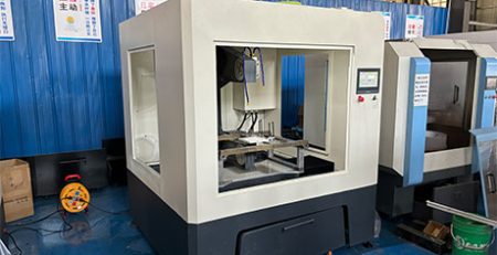
정교한 반도체 제작 세계에서, 원료 실리콘 잉곳에서 고성능 집적 회로로의 여정은 현대 공학의 경이로움이다. 이 여정의 시작에는 전체 공급망의 효율성을 결정하는 과정이 있다:실리콘 웨이퍼 절단.
우리가 2026 연등 축제를 기념하고 새로운 한 해의 “더 나은” 생산을 기대하면서, Ensoll은 고정밀 절단 솔루션을 선도하게 된 것을 자랑스럽게 생각한다. 제조업체들에게, the choice of cutting tool is no longer just a procurement decision—it is a strategic move that dictates yield, cost, and global competitiveness.
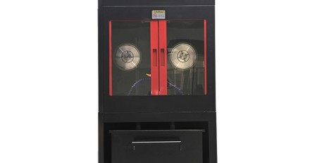
The fulldiamond wire saw cutting process— from ingot mounting to wafer cleaning — is documented step by step in our monocrystalline silicon guide.
1. The Critical Role of Silicon Wafer Cutting
Silicon remains the “bedrock” of the digital age. Whether it is Monocrystalline Silicon for high-efficiency CPUs or Polycrystalline Silicon for solar arrays, the goal of slicing is always the same: to produce thin, flat, and damage-free wafers with the least amount of material loss.
The Challenge of “The Kerf”
In the semiconductor industry, silicon is essentially “liquid gold.” When an ingot is sliced, the thickness of the cutting tool creates a gap called the kerf. The material in this gap is turned into fine dust (swarf) and lost forever. Traditional sawing methods often lose up to 30% 받는 사람 40% of the ingot to kerf loss.
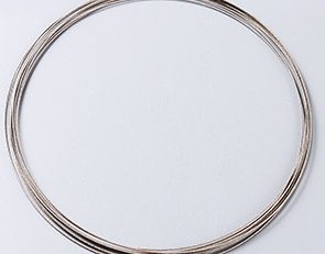
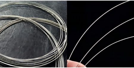
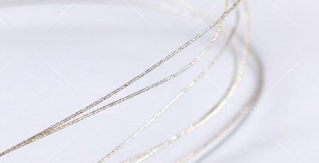
Ensoll’s다이아몬드 와이어 톱technology addresses this head-on. By utilizing ultra-thin wires (as thin as 80μm to 120μm), we minimize the “gap” and maximize the number of wafers harvested from a single ingot.
비디오 쇼케이스: High-Speed Silicon Slicing
2. Why Diamond Wire Saw Outperforms Traditional Methods
For decades, the industry relied on Slurry Wire Saws (using loose silicon carbide grit in a liquid carrier). 그렇지만, as we move into 2026, DWS has become the undisputed champion. Here is why:
A. Fixed Abrasive Efficiency
In a slurry saw, the grit “rolls” between the wire and the silicon, leading to a chaotic and slow cutting action. In an Ensoll Diamond Wire, the diamonds are electroplated directly onto the wire. This “fixed abrasive” method allows for:
Faster Linear Speeds: Reducing cutting time by up to 75%.
Lower Cutting Force: Minimizing the risk of wafer breakage.
B. Superior Surface Geometry
Semiconductor wafers must be perfectly flat. Any “bow” or “뒤틀림” can cause errors during the subsequent lithography process. Ensoll’s wire saws provide:
Unmatched TTV (총 두께 변동): Ensuring every wafer is uniform from edge to center.
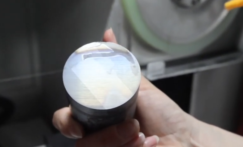
Reduced Saw Marks: A smoother surface means less time spent in the expensive Chemical Mechanical Polishing (CMP) stage.
Image Showcase: 표면 품질 비교
3. The Technical Heart of Ensoll: Our Diamond Wire Construction.
Not all diamond wires are created equal. 엔솔에서는, our R&D has perfected a proprietary electroplating process that ensures the longevity and performance of our tools.
High-Tensile Core: We use premium high-carbon steel that can withstand the extreme tension required for high-speed wafering without snapping.
Diamond Grit Selection: We use synthetic diamonds with specific crystalline shapes to ensure maximum “bite” into the silicon.
Uniform Distribution: 우리의 “더 나은” 2026 manufacturing line ensures that diamond particles are distributed with mathematical precision, preventing “bald spots” on the wire that cause uneven cuts.
4. Expanding Beyond Silicon: SiC 및 GaN
The semiconductor landscape is shifting toward Wide Bandgap (WBG) materials like Silicon Carbide (원문대로). These materials are nearly as hard as diamond itself, making them notoriously difficult to cut.
Ensoll’s diamond wire saw tools are specifically engineered for these “hard and brittle” challenges. By optimizing the bond between the diamond and the wire, we allow for the efficient slicing of SiC ingots, which is crucial for the burgeoning Electric Vehicle (EV) and 5G Power industries.
5. Environmental and Economic Impact: The Green Advantage
Sustainability is a core pillar of Ensoll’s 2026 mission. Traditional slurry sawing produces large amounts of toxic waste that is difficult to recycle.
Zero Slurry: DWS uses water-based coolants that are significantly easier to filter and recycle.
Energy Efficiency: Faster cutting times mean lower energy consumption per wafer.
Cost Reduction: By reducing kerf loss and polishing time, Ensoll helps manufacturers lower their Cost Per Wafer significantly.
6. Ensoll’s 2026 Service Guarantee: Our Three Promises
As highlighted in our Lantern Festival commencement, we are not just providing tools; we are providing a “Fullfillment” package:
정밀 이행: We guarantee that our wires will maintain consistent diameters throughout their lifespan, ensuring stable yields.
Service Fulfillment: Our Global 4-hour response team is active in every major tech hub (from Singapore to the UAE) to troubleshoot and optimize your lines.
Partnership Fulfillment: We work with your engineers to customize wire specifications for your specific ingot sizes and machine types.
Silicon wafer cutting is the first cost-defining step in semiconductor fabrication: kerf loss directly sets how many wafers one ingot yields.
Diamond wire saw outperforms ID blades and slurry saws because fixed diamond abrasive gives a narrower kerf, better surface geometry and less material waste.
Ensoll diamond wire combines electroplated diamond grit with high-tensile steel wire, keeping tension stable and wire life long in production slicing.
The same diamond wire platform extends beyond silicon to SiC and GaN substrates with adjusted speed, tension and coolant parameters.
결론: 이 “더 나은” Way to Cut
The semiconductor industry moves at light speed, and your cutting technology must keep pace. Silicon Wafer Cutting is the foundation upon which all modern technology is built. By partnering with Ensoll and utilizing our advanced Diamond Wire Saw solutions, you are choosing a path of higher efficiency, lower waste, and superior precision.
As we light the lanterns for 2026, let us light the way for your production line. Experience the “정밀 이행” that only Ensoll can provide.
자주 묻는 질문
Why is diamond wire saw the standard for silicon wafer cutting?
Fixed diamond abrasive cuts with a narrow kerf (일반적으로 120-250 μm의), holds tight TTV and wastes far less silicon than ID blades or slurry sawing, so more wafers are produced per ingot.
What is kerf loss and why does it matter?
Kerf loss is the width of material removed by the cut. Every micrometer saved means more wafers per ingot, which is the dominant cost lever in silicon wafer production.
Can the same diamond wire saw cut SiC and GaN?
예. Diamond wire handles hard, brittle materials well; only process parameters such as wire speed, tension and coolant need to be adjusted for each material.
What surface quality does diamond wire cutting achieve?
As-cut surfaces typically reach Ra 0.2-0.5 µm with minimal sub-surface damage, which shortens downstream lapping and polishing time.
엔솔 엔지니어링 팀이 검토한 기술 내용 — 다이아몬드 와이어 루프 제조업체 10+ 다년간의 생산 경험을 가진 회사.